MICROFC-SMTPA-10035-GEVB
onsemi
Evaluation Board, MicroFC-10035 SiPM Sensor, 3 x Through Hole Pins, Bias Voltage
8T49N241-EVK
Renesas Electronics Corporation
Evaluation Kit, 8T49N2421, Frequency Translator, Clock & Timing
5P49V60-EVK
Renesas Electronics Corporation
Evaluation Board, 5P49V60 Programmable Clock Generator, VersaClock 6E, Automotive

| Distributor | SKU | Stock | MOQ | 1 | 10 | 50 | 100 | 1,000 | 10,000 |
|---|---|---|---|---|---|---|---|---|---|
| DigiKey | 296-37772-ND | 1 | 1 | $454.30 | $454.30 | $454.30 | $454.30 | $454.30 | $454.30 |
| Arrow Asia | TMDSEMU200-U | 0 | 1 | $345.10 | $319.85 | $319.85 | $319.85 | $319.85 | $319.85 |
| Arrow North American Components | TMDSEMU200-U | 0 | 1 | $405.33 | $401.28 | $393.29 | $389.36 | $377.80 | $374.02 |
| AVNET Asia Pacific | TMDSEMU200-U | 0 | 1 | $0.00 | $0.00 | $0.00 | $0.00 | $0.00 | $0.00 |
| AVNET Europe | TMDSEMU200-U | 0 | 1 | * $445.55 | * $427.73 | * $392.08 | * $378.72 | * $378.72 | * $378.72 |
| AVNET Express | TMDSEMU200-U | 0 | 1 | $359.90 | $359.90 | $359.90 | $359.90 | $359.90 | $359.90 |
| element14 APAC | TMDSEMU200-U | 1 | 1 | * $436.42 | * $436.42 | * $436.42 | * $436.42 | * $436.42 | * $436.42 |
| Farnell | TMDSEMU200-U | 3 | 1 | * $445.53 | * $445.53 | * $445.53 | * $445.53 | * $445.53 | * $445.53 |
| Mouser Electronics | 595-TMDSEMU200-U | 110 | 1 | $392.36 | $392.35 | $392.35 | $392.35 | $392.35 | $392.35 |
| Newark | TMDSEMU200-U | 5 | 1 | $324.50 | $324.50 | $324.50 | $324.50 | $324.50 | $324.50 |
| RS Components | TMDSEMU200-U | 0 | $457.61 | ||||||
| Texas Instruments | TMDSEMU200-U | 200 | 1 | $295.00 | $295.00 | $295.00 | $295.00 | $295.00 | $295.00 |
| Verical Marketplace | TMDSEMU200-U | 103 | 1 | $303.74 | $355.30 | $345.95 | $341.46 | $306.42 | $306.42 |
| Win Source | TMDSEMU200-U | 14 | 1 |
| Distributor | SKU | Stock | MOQ | 1 | 10 | 50 | 100 | 1,000 | 10,000 |
|---|---|---|---|---|---|---|---|---|---|
| DigiKey | 296-31026-ND | 0 | 1 | $105.96 | $105.96 | $105.96 | $105.96 | $105.96 | $105.96 |
| element14 APAC | TLK100INTEVM | 0 | $1.00 | ||||||
| Farnell | TLK100INTEVM | 0 | * $135.13 | ||||||
| Mouser Electronics | 595-TLK100INTEVM | 0 | 1 | $0.00 | |||||
| Newark | TLK100INTEVM | 0 | 1 | $98.94 | $98.94 | $98.94 | $98.94 | $98.94 | $98.94 |
| Texas Instruments | TLK100INTEVM | 11 | 1 | $99.00 | $99.00 | $99.00 | $99.00 | $99.00 | $99.00 |
| Distributor | SKU | Stock | MOQ | 1 | 10 | 50 | 100 | 1,000 | 10,000 |
|---|---|---|---|---|---|---|---|---|---|
| DigiKey | STEVAL-ISQ013V1 | 0 | 1 | $26.25 | |||||
| Ameya360 | STEVAL-ISQ013V1 | 5 | $34.13 | ||||||
| AVNET Express | STEVAL-ISQ013V1 | 0 | 1 | $26.58 | |||||
| element14 APAC | STEVAL-ISQ013V1 | 1 | 24 | $40.40 | |||||
| Farnell | STEVAL-ISQ013V1 | 1 | 1 | $24.17 | |||||
| Future Electronics | STEVAL-ISQ013V1 | 5 | 1 | $25.35 | |||||
| Mouser Electronics | STEVAL-ISQ013V1 | 9 | 1 | ||||||
| Newark | STEVAL-ISQ013V1 | 1 | 24 | $26.25 | |||||
| Utsource | STEVAL-ISQ013V1 | 33951 | $41.69 | ||||||
| Win Source | STEVAL-ISQ013V1 | 1700 |
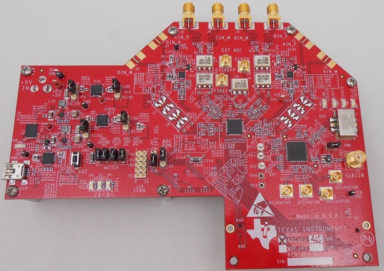
ADC32J25 Dual-Channel; 12-Bit; 160-MSPS Analog-to-Digital Converter Evaluation Module
Texas Instruments
ADC32J25 Dual-Channel; 12-Bit; 160-MSPS Analog-to-Digital Converter Evaluation Module
| Distributor | SKU | Stock | MOQ | 1 | 10 | 50 | 100 | 1,000 | 10,000 |
|---|---|---|---|---|---|---|---|---|---|
| DigiKey | 296-42189-ND | 2 | 1 | $358.80 | $358.80 | $358.80 | $358.80 | $358.80 | $358.80 |
| Arrow North American Components | ADC32J25EVM | 0 | 1 | $399.12 | $395.13 | $0.00 | $383.39 | $372.01 | $303.12 |
| AVNET Express | ADC32J25EVM | 0 | 1 | $364.78 | $364.78 | $364.78 | $364.78 | $364.78 | $364.78 |
| Mouser Electronics | 595-ADC32J25EVM | 0 | 1 | $397.69 | $397.69 | $397.69 | $397.69 | $397.69 | $397.69 |
| Texas Instruments | ADC32J25EVM | 12 | 1 | $299.00 | $299.00 | $299.00 | $299.00 | $299.00 | $299.00 |
| Verical Marketplace | ADC32J25EVM | 5 | 1 | $427.14 | $0.00 | $0.00 | $0.00 | $0.00 | $0.00 |
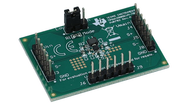
TPS610985 Ultra Low Quiescent Current Boost Evaluation Module
Texas Instruments
TPS610985 Ultra Low Quiescent Current Boost Evaluation Module
| Distributor | SKU | Stock | MOQ | 1 | 10 | 50 | 100 | 1,000 | 10,000 |
|---|---|---|---|---|---|---|---|---|---|
| DigiKey | 296-44006-ND | 1 | 1 | $61.25 | $61.25 | $61.25 | $61.25 | $61.25 | $61.25 |
| Arrow North American Components | TPS610985EVM-782 | 0 | 1 | $66.57 | $65.90 | $64.59 | $63.94 | $62.04 | $61.42 |
| AVNET Express | TPS610985EVM-782 | 0 | 1 | $59.78 | $59.78 | $59.78 | $59.78 | $59.78 | $59.78 |
| Mouser Electronics | 595-TPS610985EVM-782 | 0 | 1 | $64.85 | $64.85 | $64.85 | $64.85 | $64.85 | $64.85 |
| Newark | TPS610985EVM-782 | 0 | 1 | $50.73 | $50.73 | $50.73 | $50.73 | $50.73 | $50.73 |
| Texas Instruments | TPS610985EVM-782 | 15 | 1 | $49.00 | $49.00 | $49.00 | $49.00 | $49.00 | $49.00 |
| Verical Marketplace | TPS610985EVM-782 | 17 | 1 | $50.73 | $0.00 | $0.00 | $0.00 | $0.00 | $0.00 |
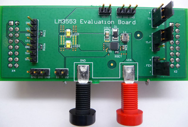
1.2A Dual Flash LED Driver System with I2C Compatible Interface
Texas Instruments
1.2A Dual Flash LED Driver System with I2C Compatible Interface
| Distributor | SKU | Stock | MOQ | 1 | 10 | 50 | 100 | 1,000 | 10,000 |
|---|---|---|---|---|---|---|---|---|---|
| DigiKey | LM3553SDEV-ND | 1 | 1 | $178.80 | $178.80 | $178.80 | $178.80 | $178.80 | $178.80 |
| Arrow North American Components | LM3553SDEV | 0 | 1 | $202.71 | $200.69 | $196.69 | $194.73 | $188.94 | $187.05 |
| AVNET Express | LM3553SDEV | 0 | 1 | $181.78 | $181.78 | $181.78 | $181.78 | $181.78 | $181.78 |
| element14 APAC | LM3553SDEV | 1 | 1 | * $251.22 | * $251.22 | * $251.22 | * $251.22 | * $251.22 | * $251.22 |
| Farnell | LM3553SDEV | 1 | 1 | * $198.96 | * $198.96 | * $198.96 | * $198.96 | * $198.96 | * $198.96 |
| Mouser Electronics | 926-LM3553SDEV | 0 | 1 | $193.72 | $193.72 | $193.72 | $193.72 | $193.72 | $193.72 |
| Newark | LM3553SDEV | 1 | 1 | $153.41 | $153.41 | $153.41 | $153.41 | $153.41 | $153.41 |
| Texas Instruments | LM3553SDEV | 23 | 1 | $149.00 | $149.00 | $149.00 | $149.00 | $149.00 | $149.00 |
| Verical Marketplace | LM3553SDEV | 4 | 1 | $212.86 | $172.43 | $172.43 | $172.43 | $172.43 | $172.43 |