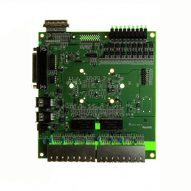
KSZ8999-EVAL
Microchip Technology Inc.
Ethernet Development Tools KSZ899 Eval, No Power Supply Incl.
| Distributor | SKU | Stock | MOQ | 1 | 10 | 50 | 100 | 1,000 | 10,000 |
|---|---|---|---|---|---|---|---|---|---|
| AVNET Europe | KSZ8999-EVAL | 0 | 1 | * $0.00 | * $0.00 | * $0.00 | * $0.00 | * $0.00 | * $0.00 |
| MicrochipDirect | KSZ8999-EVAL | 1 | $305.00 | $305.00 | $305.00 | $305.00 | $305.00 | $305.00 | |
| Mouser Electronics | 998-KSZ8999-EVAL | 1 | 1 | $426.65 | $426.65 | $426.65 | $426.65 | $426.65 | $426.65 |
| Win Source | KSZ8999-EVAL | 4510 |
STEVAL-55G0MBI1
STMicroelectronics
Hardware MIPI CSI-2 kit integrating VD55G0 sensor embedded processing platform
STEVAL-56G3MAI1
STMicroelectronics
Hardware MIPI CSI-2 kit integrating VD56G3 sensor embedded processing platform
STEVAL-EVK-U0I1
STMicroelectronics
EVK Main Hardware USB kit For Evaluating ST Bright Sense Image Sensor
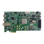
MPF300-EVAL-KIT
Microchip Technology Inc.
Programmable Logic IC Development Tools PolarFire Eval Kit
| Distributor | SKU | Stock | MOQ | 1 | 10 | 50 | 100 | 1,000 | 10,000 |
|---|---|---|---|---|---|---|---|---|---|
| DigiKey | MPF300-EVAL-KIT-ES-ND | 0 | 1 | $1,562.50 | $1,562.50 | $1,562.50 | $1,562.50 | $1,562.50 | $1,562.50 |
| Arrow North American Components | MPF300-EVAL-KIT | 2 | 1 | $1,902.51 | $1,493.51 | $1,493.51 | $1,460.80 | $1,449.95 | $1,449.95 |
| AVNET Europe | MPF300-EVAL-KIT | 0 | 1 | * $0.00 | * $0.00 | * $0.00 | * $0.00 | * $0.00 | * $0.00 |
| AVNET Express | MPF300-EVAL-KIT | 2 | 1 | $1,776.54 | $0.00 | $0.00 | $0.00 | $0.00 | $0.00 |
| Farnell | MPF300-EVAL-KIT | 15 | 1 | * $1,937.75 | * $1,937.75 | * $1,937.75 | * $1,937.75 | * $1,937.75 | * $1,937.75 |
| Mouser Electronics | 494-MPF300-EVAL-KIT | 41 | 1 | $1,962.32 | $1,962.32 | $1,962.32 | $1,962.32 | $1,962.32 | $1,962.32 |