A Single-Phase, D-CAP+? Synchronous Buck Controller for Intel Core? i3, i5, i7 Applications
Texas Instruments
A Single-Phase, D-CAP+? Synchronous Buck Controller for Intel Core? i3, i5, i7 Applications
| Distributor | SKU | Stock | MOQ | 1 | 10 | 50 | 100 | 1,000 | 10,000 |
|---|---|---|---|---|---|---|---|---|---|
| DigiKey | TPS59611EVM-622-ND | 0 | 1 | $0.00 | $0.00 | $0.00 | $0.00 | $0.00 | $0.00 |
| AVNET Express | TPS59611EVM-622 | 0 | 1 | $0.00 | $0.00 | $0.00 | $0.00 | $0.00 | $0.00 |
| Mouser Electronics | 595-TPS59611EVM-622 | 0 | 1 | $0.00 | |||||
| Texas Instruments | TPS59611EVM-622 | 236 | $49.00 |
| Distributor | SKU | Stock | MOQ | 1 | 10 | 50 | 100 | 1,000 | 10,000 |
|---|---|---|---|---|---|---|---|---|---|
| DigiKey | 296-29086-ND | 0 | 1 | $186.25 | $186.25 | $186.25 | $186.25 | $186.25 | $186.25 |
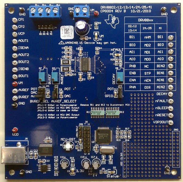
| Arrow North American Components | DRV8840EVM | 0 | 1 | $202.00 | $199.98 | $196.00 | $194.04 | $188.28 | $151.28 |
| AVNET Europe | DRV8840EVM | 0 | 1 | * $192.12 | * $189.65 | * $184.94 | * $182.59 | * $182.59 | * $182.59 |
| AVNET Express | DRV8840EVM | 0 | 1 | $181.78 | $181.78 | $181.78 | $181.78 | $181.78 | $181.78 |
| element14 APAC | DRV8840EVM | 1 | 1 | * $221.44 | * $221.44 | * $221.44 | * $221.44 | * $221.44 | * $221.44 |
| Farnell | DRV8840EVM | 1 | 1 | * $226.38 | * $226.38 | * $226.38 | * $226.38 | * $226.38 | * $226.38 |
| Mouser Electronics | 595-DRV8840EVM | 1 | 1 | $193.72 | $193.72 | $193.72 | $193.72 | $193.72 | $193.72 |
| Newark | DRV8840EVM | 0 | 1 | $191.88 | $191.88 | $191.88 | $191.88 | $191.88 | $191.88 |
| Texas Instruments | DRV8840EVM | 10 | 1 | $149.00 | $149.00 | $149.00 | $149.00 | $149.00 | $149.00 |
| Verical Marketplace | DRV8840EVM | 1 | 1 | $206.79 | $206.79 | $206.79 | $206.79 | $206.79 | $206.79 |
Hercules RM46x controlCARD for motor control development kits
Texas Instruments
Hercules RM46x controlCARD for motor control development kits
| Distributor | SKU | Stock | MOQ | 1 | 10 | 50 | 100 | 1,000 | 10,000 |
|---|---|---|---|---|---|---|---|---|---|
| DigiKey | 296-35080-ND | 0 | 1 | $163.90 | $163.90 | $163.90 | $163.90 | $163.90 | $163.90 |
| AVNET Express | TMDXRM46CNCD | 0 | 1 | $0.00 | $0.00 | $0.00 | $0.00 | $0.00 | $0.00 |
| element14 APAC | TMDXRM46CNCD | 0 | 1 | * $186.56 | * $186.56 | * $186.56 | * $186.56 | * $186.56 | * $186.56 |
| Farnell | TMDXRM46CNCD | 0 | 1 | * $189.34 | * $189.34 | * $189.34 | * $189.34 | * $189.34 | * $189.34 |
| Mouser Electronics | 595-TMDXRM46CNCD | 0 | 1 | $0.00 | |||||
| Newark | TMDXRM46CNCD | 1 | 1 | $153.41 | $153.41 | $153.41 | $153.41 | $153.41 | $153.41 |
| Texas Instruments | TMDXRM46CNCD | 51 | $149.00 |
Stellaris? LM4F120 LaunchPad Evaluation Board Software
Texas Instruments
Stellaris? LM4F120 LaunchPad Evaluation Board Software
| Distributor | SKU | Stock | MOQ | 1 | 10 | 50 | 100 | 1,000 | 10,000 |
|---|---|---|---|---|---|---|---|---|---|
| Mouser Electronics | N/A | 0 |
| Distributor | SKU | Stock | MOQ | 1 | 10 | 50 | 100 | 1,000 | 10,000 |
|---|---|---|---|---|---|---|---|---|---|
| DigiKey | 296-30844-ND | 0 | 1 | $163.90 | $163.90 | $163.90 | $163.90 | $163.90 | $163.90 |
| Arrow North American Components | CDCLVP1212EVM | 0 | 1 | $157.34 | $156.75 | $156.75 | $153.52 | $152.09 | $152.09 |
| AVNET Express | CDCLVP1212EVM | 0 | 1 | $0.00 | $0.00 | $0.00 | $0.00 | $0.00 | $0.00 |
| Mouser Electronics | 595-CDCLVP1212EVM | 0 | 1 | ||||||
| Newark | CDCLVP1212EVM | 1 | 1 | $19.09 | $19.09 | $19.09 | $19.09 | $19.09 | $19.09 |
| Texas Instruments | CDCLVP1212EVM | 1 | 1 | $149.00 | $149.00 | $149.00 | $149.00 | $149.00 | $149.00 |
| Verical Marketplace | CDCLVP1212EVM | 1 | 1 | $187.31 | $0.00 | $0.00 | $0.00 | $0.00 | $0.00 |
Evaluation Module for TPS65735, PMU for Active Shutter 3D Glasses
Texas Instruments
Evaluation Module for TPS65735, PMU for Active Shutter 3D Glasses
| Distributor | SKU | Stock | MOQ | 1 | 10 | 50 | 100 | 1,000 | 10,000 |
|---|---|---|---|---|---|---|---|---|---|
| DigiKey | 296-45963-ND | 0 | |||||||
| Arrow North American Components | TPS65735EVM-703 | 0 | 1 | $0.00 | $0.00 | $0.00 | $0.00 | $0.00 | $0.00 |
| AVNET Express | TPS65735EVM-703 | 0 | 1 | $0.00 | $0.00 | $0.00 | $0.00 | $0.00 | $0.00 |
| element14 APAC | TPS65735EVM-703 | 3 | 1 | * $61.14 | * $61.14 | * $61.14 | * $61.14 | * $61.14 | * $61.14 |
| Farnell | TPS65735EVM-703 | 3 | 1 | * $50.97 | * $50.97 | * $50.97 | * $50.97 | * $50.97 | * $50.97 |
| Mouser Electronics | 595-TPS65735EVM-703 | 1 | 1 | $57.35 | $57.34 | $57.34 | $57.34 | $57.34 | $57.34 |
| Newark | TPS65735EVM-703 | 0 | 1 | $0.00 | $0.00 | $0.00 | $0.00 | $0.00 | $0.00 |
| Texas Instruments | TPS65735EVM-703 | 66 | 1 | $49.00 | $49.00 | $49.00 | $49.00 | $49.00 | $49.00 |
| Verical Marketplace | TPS65735EVM-703 | 40 | 1 | $62.38 | $0.00 | $0.00 | $0.00 | $0.00 | $0.00 |
Thin SOT23 1A Load Step-Down DC-DC Regulator Evaluation Module
Texas Instruments
Thin SOT23 1A Load Step-Down DC-DC Regulator Evaluation Module
| Distributor | SKU | Stock | MOQ | 1 | 10 | 50 | 100 | 1,000 | 10,000 |
|---|---|---|---|---|---|---|---|---|---|
| DigiKey | LM2734XEVAL-ND | 3 | $199.00 | $199.00 | $199.00 | $199.00 | $199.00 | $199.00 | |
| Verical Marketplace | LM2734X EVAL | 22 | 1 | $65.18 | $65.18 | $65.18 | $65.18 | $65.18 | $65.18 |
THS4211 Evaluation Module with Unity Gain
Texas Instruments
THS4211 Evaluation Module with Unity Gain
| Distributor | SKU | Stock | MOQ | 1 | 10 | 50 | 100 | 1,000 | 10,000 |
|---|---|---|---|---|---|---|---|---|---|
| DigiKey | 296-20550-ND | 0 | 1 | $61.25 | $61.25 | $61.25 | $61.25 | $61.25 | $61.25 |
| Arrow North American Components | THS4211EVM-UG | 0 | 1 | $57.31 | $50.65 | $50.65 | $50.16 | $0.00 | $0.00 |
| AVNET Europe | THS4211EVM-UG | 0 | 1 | * $69.45 | * $67.33 | * $63.56 | * $61.80 | * $61.80 | * $61.80 |
| AVNET Express | THS4211EVM-UG | 0 | 1 | $59.78 | $59.78 | $59.78 | $59.78 | $59.78 | $59.78 |
| Mouser Electronics | 595-THS4211EVM-UG | 0 | 1 | $64.85 | $64.84 | $64.84 | $64.84 | $64.84 | $64.84 |
| Texas Instruments | THS4211EVM-UG | 25 | 1 | $49.00 | $49.00 | $49.00 | $49.00 | $49.00 | $49.00 |
| Verical Marketplace | THS4211EVM-UG | 25 | 1 | $63.41 | $59.89 | $59.07 | $59.07 | $59.07 | $59.07 |
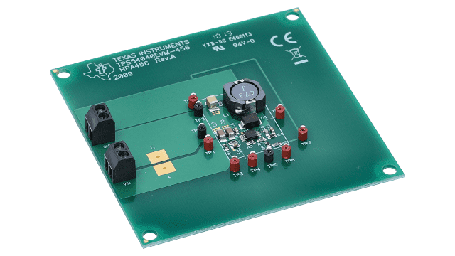
TPS54040 42V Input; 5V Output; 0.5A Evaluation Module
Texas Instruments
TPS54040 42V Input; 5V Output; 0.5A Evaluation Module
| Distributor | SKU | Stock | MOQ | 1 | 10 | 50 | 100 | 1,000 | 10,000 |
|---|---|---|---|---|---|---|---|---|---|
| DigiKey | 296-31177-ND | 2 | 1 | $30.00 | $30.00 | $30.00 | $30.00 | $30.00 | $30.00 |
| Arrow North American Components | TPS54040EVM-456 | 0 | 1 | $28.85 | $29.45 | $29.45 | $29.17 | $0.00 | $0.00 |
| AVNET Europe | TPS54040EVM-456 | 0 | 1 | * $39.43 | * $37.43 | * $34.01 | * $32.48 | * $32.48 | * $32.48 |
| AVNET Express | TPS54040EVM-456 | 0 | 1 | $30.50 | $30.50 | $30.50 | $30.50 | $30.50 | $30.50 |
| element14 APAC | TPS54040EVM-456 | 1 | 1 | * $32.42 | * $32.42 | * $32.42 | * $32.42 | * $32.42 | * $32.42 |
| Farnell | TPS54040EVM-456 | 1 | 1 | * $37.99 | * $37.99 | * $37.99 | * $37.99 | * $37.99 | * $37.99 |
| Mouser Electronics | 595-TPS54040EVM-456 | 2 | 1 | $33.24 | $33.24 | $33.24 | $33.24 | $33.24 | $33.24 |
| Newark | TPS54040EVM-456 | 1 | 1 | $33.38 | $32.60 | $32.60 | $32.60 | $32.60 | $32.60 |
| Texas Instruments | TPS54040EVM-456 | 26 | 1 | $25.00 | $25.00 | $25.00 | $25.00 | $25.00 | $25.00 |
| Verical Marketplace | TPS54040EVM-456 | 9 | 1 | $25.95 | $28.24 | $28.24 | $28.24 | $28.24 | $28.24 |
| Distributor | SKU | Stock | MOQ | 1 | 10 | 50 | 100 | 1,000 | 10,000 |
|---|---|---|---|---|---|---|---|---|---|
| DigiKey | 296-52572-ND | 2 | 1 | $104.54 | $104.54 | $104.54 | $104.54 | $104.54 | $104.54 |
| AVNET Express | TSC2008EVM | 0 | 1 | $0.00 | $0.00 | $0.00 | $0.00 | $0.00 | $0.00 |
| Mouser Electronics | 595-TSC2008EVM | 0 | 1 | $0.00 | |||||
| Texas Instruments | TSC2008EVM | 19 | $49.00 |