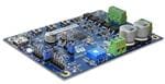
STEVAL-SPIN3201
STMicroelectronics
Power Management IC Development Tools STSPIN32F0 Advanced BLDC controller with embedded STM32 MCU evaluation board
| Distributor | SKU | Stock | MOQ | 1 | 10 | 50 | 100 | 1,000 | 10,000 |
|---|---|---|---|---|---|---|---|---|---|
| DigiKey | 497-16988-ND | 0 | 1 | $62.16 | $62.16 | $62.16 | $62.16 | $62.16 | $62.16 |
| Ameya360 | STEVAL-SPIN3201 | 6 | $78.00 | $78.00 | $78.00 | $78.00 | $78.00 | $78.00 | |
| Anglia | STEVAL-SPIN3201 | 3 | |||||||
| Arrow Europe | STEVAL-SPIN3201 | 0 | 1 | $58.08 | $58.08 | $58.08 | $58.08 | $58.08 | $58.08 |
| Arrow North American Components | STEVAL-SPIN3201 | 0 | 11 | $62.26 | $61.11 | $54.57 | $54.05 | $56.89 | $55.17 |
| AVNET Asia Pacific | STEVAL-SPIN3201 | 0 | 1 | $0.00 | $0.00 | $0.00 | $0.00 | $0.00 | $0.00 |
| AVNET Europe | STEVAL-SPIN3201 | 1 | 1 | * $262.35 | * $243.34 | * $186.31 | * $168.82 | * $168.82 | * $168.82 |
| AVNET Express | STEVAL-SPIN3201 | 12 | 1 | $61.70 | $60.18 | $59.09 | $58.03 | $58.03 | |
| element14 APAC | STEVAL-SPIN3201 | 16 | 1 | * $88.27 | * $88.27 | * $88.27 | * $88.27 | * $88.27 | * $88.27 |
| Farnell | STEVAL-SPIN3201 | 20 | 1 | * $80.56 | * $80.56 | * $80.56 | * $80.56 | * $80.56 | * $80.56 |
| Future Electronics | STEVAL-SPIN3201 | 4 | 1 | $82.05 | $61.54 | $61.54 | $61.54 | $61.54 | $61.54 |
| Jak Electronics | STEVAL-SPIN3201 | 0 | $734.77 | $734.77 | $734.77 | $734.77 | $734.77 | $0.00 | |
| Mouser Electronics | 511-STEVAL-SPIN3201 | 6 | 1 | $71.02 | $71.02 | $71.02 | $71.02 | $71.02 | $71.02 |
| Newark | STEVAL-SPIN3201 | 3 | 1 | $79.76 | $79.76 | $79.76 | $79.76 | $79.76 | $79.76 |
| RS Components | STEVAL-SPIN3201 | 0 | $64.68 | ||||||
| RS Components (APAC) | STEVAL-SPIN3201 | 0 | $138.83 | ||||||
| Utmel | STEVAL-SPIN3201 | 0 | $99.72 | $99.72 | $99.72 | $99.72 | $99.72 | $0.00 | |
| Verical Marketplace | STEVAL-SPIN3201 | 12 | 1 | $63.78 | $0.00 | $0.00 | $0.00 | $0.00 | $0.00 |
| Win Source | STEVAL-SPIN3201 | 470 | 1 |
| Distributor | SKU | Stock | MOQ | 1 | 10 | 50 | 100 | 1,000 | 10,000 |
|---|---|---|---|---|---|---|---|---|---|
| Mouser Electronics | 667-EVAL-PAN4561 | 0 | 10 | $192.03 | $192.03 | $192.03 | $192.03 | $192.03 |
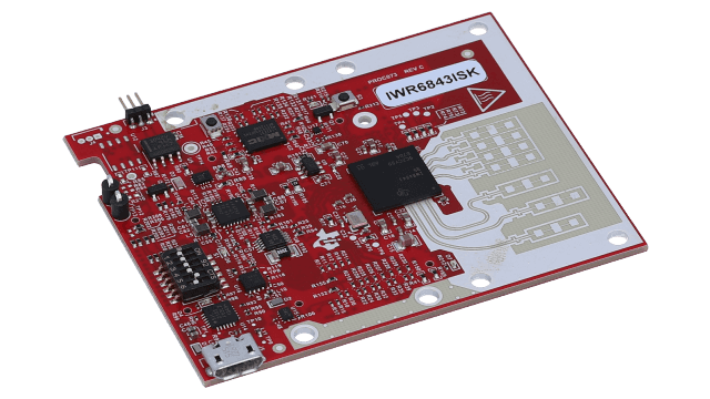
IWR6843 intelligent mmWave sensor standard antenna plug-in module
Texas Instruments
IWR6843 intelligent mmWave sensor standard antenna plug-in module
| Distributor | SKU | Stock | MOQ | 1 | 10 | 50 | 100 | 1,000 | 10,000 |
|---|---|---|---|---|---|---|---|---|---|
| DigiKey | 296-IWR6843ISK-ODS-ND | 6 | 1 | $210.00 | $210.00 | $210.00 | $210.00 | $210.00 | $210.00 |
| Arrow North American Components | IWR6843ISK | 0 | 1 | $237.85 | $235.47 | $230.78 | $228.47 | $221.69 | $219.47 |
| AVNET Express | IWR6843ISK | 0 | 1 | $164.70 | $164.70 | $164.70 | $164.70 | $164.70 | $164.70 |
| Mouser Electronics | 595-IWR6843ISK | 85 | 1 | $232.75 | $232.75 | $232.75 | $232.75 | $232.75 | $232.75 |
| Texas Instruments | IWR6843ISK | 1165 | 1 | $175.00 | $175.00 | $175.00 | $175.00 | $175.00 | $175.00 |
| Verical Marketplace | IWR6843ISK | 136 | 1 | $161.99 | $161.99 | $161.99 | $161.99 | $161.99 | $161.99 |
| Distributor | SKU | Stock | MOQ | 1 | 10 | 50 | 100 | 1,000 | 10,000 |
|---|---|---|---|---|---|---|---|---|---|
| AVNET Asia Pacific | TMDX654GPEVM | 0 | 1 | $0.00 | $0.00 | $0.00 | $0.00 | $0.00 | $0.00 |
| AVNET Express | TMDX654GPEVM | 0 | 1 | $0.00 | $0.00 | $0.00 | $0.00 | $0.00 | $0.00 |
| Mouser Electronics | 595-TMDX654GPEVM | 0 | 1 | ||||||
| Texas Instruments | TMDX654GPEVM | 126 | 1 | $699.00 | $699.00 | $699.00 | $699.00 | $699.00 | $699.00 |
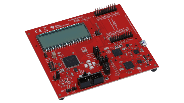
MSP430FR6047 ultrasonic sensing evaluation module
Texas Instruments
MSP430FR6047 ultrasonic sensing evaluation module
| Distributor | SKU | Stock | MOQ | 1 | 10 | 50 | 100 | 1,000 | 10,000 |
|---|---|---|---|---|---|---|---|---|---|
| DigiKey | 296-49383-ND | 34 | 1 | $210.00 | $210.00 | $210.00 | $210.00 | $210.00 | $210.00 |
| AVNET Europe | EVM430-FR6047 | 0 | 1 | * $411.14 | * $390.71 | * $362.62 | * $352.41 | * $352.41 | * $352.41 |
| AVNET Express | EVM430-FR6047 | 0 | 1 | $303.78 | $303.78 | $303.78 | $303.78 | $303.78 | $303.78 |
| Mouser Electronics | 595-EVM430-FR6047 | 15 | 1 | $232.75 | $232.75 | $232.75 | $232.75 | $232.75 | $232.75 |
| Texas Instruments | EVM430-FR6047 | 111 | 1 | $175.00 | $175.00 | $175.00 | $175.00 | $175.00 | $175.00 |
| Win Source | EVM430-FR6047 | 1 | 1 |
STEVAL-MKI184V1
STMicroelectronics
Acceleration Sensor Development Tools ISM303DAC adapter board for a standard DIL24 socket
| Distributor | SKU | Stock | MOQ | 1 | 10 | 50 | 100 | 1,000 | 10,000 |
|---|---|---|---|---|---|---|---|---|---|
| DigiKey | 497-17813-ND | 5 | 1 | $18.45 | $18.45 | $18.45 | $18.45 | $18.45 | $18.45 |
| Ameya360 | STEVAL-MKI184V1 | 10 | $22.30 | $22.30 | $22.30 | $22.30 | $22.30 | $22.30 | |
| Arrow Europe | STEVAL-MKI184V1 | 29 | 1 | $8.17 | $8.17 | $8.17 | $8.17 | $8.17 | $8.17 |
| Arrow North American Components | STEVAL-MKI184V1 | 0 | 1 | $0.00 | $0.00 | $0.00 | $0.00 | $0.00 | $0.00 |
| AVNET Europe | STEVAL-MKI184V1 | 5 | 1 | * $47.87 | * $44.40 | * $34.00 | * $30.80 | * $30.80 | * $30.80 |
| element14 APAC | STEVAL-MKI184V1 | 1 | 1 | * $20.14 | * $19.74 | * $19.74 | * $19.74 | * $19.74 | * $19.74 |
| Farnell | STEVAL-MKI184V1 | 1 | 1 | * $18.58 | * $18.58 | * $18.58 | * $18.58 | * $18.58 | * $18.58 |
| Future Electronics | STEVAL-MKI184V1 | 5 | 1 | $17.15 | $17.15 | $17.15 | $17.15 | $17.15 | $17.15 |
| Mouser Electronics | 511-STEVAL-MKI184V1 | 30 | 1 | $18.61 | $18.61 | $18.61 | $18.61 | $18.61 | $18.61 |
| Newark | STEVAL-MKI184V1 | 1 | 1 | $18.45 | $18.45 | $18.45 | $18.45 | $18.45 | $18.45 |
| RS Components | STEVAL-MKI184V1 | 0 | $18.32 | ||||||
| Verical Marketplace | STEVAL-MKI184V1 | 29 | 1 | $8.17 | $8.17 | $8.17 | $8.17 | $8.17 | $8.17 |
| Win Source | STEVAL-MKI184V1 | 2600 |
ISL8240MEVAL4Z
Renesas Electronics Corporation
Power Management IC Development Tools 20A Step Down Power Supply Module Eval
| Distributor | SKU | Stock | MOQ | 1 | 10 | 50 | 100 | 1,000 | 10,000 |
|---|---|---|---|---|---|---|---|---|---|
| DigiKey | ISL8240MEVAL4Z-ND | 1 | 1 | $482.40 | $482.40 | $482.40 | $482.40 | $482.40 | $482.40 |
| AVNET Europe | ISL8240MEVAL4Z | 0 | 1 | * $286.28 | * $265.53 | * $203.30 | * $184.21 | * $184.21 | * $184.21 |
| AVNET Express | ISL8240MEVAL4Z | 0 | 1 | $0.00 | $0.00 | $0.00 | $0.00 | $0.00 | $0.00 |
| Future Electronics | ISL8240MEVAL4Z | 1 | 1 | $94.59 | $94.59 | $94.59 | $94.59 | $94.59 | $94.59 |
| Mouser Electronics | 968-ISL8240MEVAL4Z | 0 | 1 | ||||||
| Newark | ISL8240MEVAL4Z | 0 | 1 | $0.00 | $0.00 | $0.00 | $0.00 | $0.00 | $0.00 |
| Distributor | SKU | Stock | MOQ | 1 | 10 | 50 | 100 | 1,000 | 10,000 |
|---|---|---|---|---|---|---|---|---|---|
| Mouser Electronics | N/A | 0 |
| Distributor | SKU | Stock | MOQ | 1 | 10 | 50 | 100 | 1,000 | 10,000 |
|---|---|---|---|---|---|---|---|---|---|
| Mouser Electronics | N/A | 0 |
| Distributor | SKU | Stock | MOQ | 1 | 10 | 50 | 100 | 1,000 | 10,000 |
|---|---|---|---|---|---|---|---|---|---|
| Future Electronics | STEVAL-MKI185V1 | 10 | 1 | $15.69 | $15.69 | $15.69 | $15.69 | $15.69 | $15.69 |