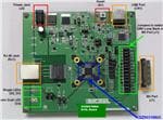
EVAL-ADG884EBZ

Analog Devices Inc.
The ADG884 is a low voltage CMOS device containing two independently selectable single-pole, double-throw (SPDT) switches. This device offers ultralow on resistance of 0.41 ? over the full temperature range, making the part an ideal solution for applications that require minimal distortion through the switch. The ADG884 also has the capability of carrying large amounts of current, typically 600 mA at 5 V operation.The ADG884 is available in a 10-ball, 2 mm ? 1.5 mm WLCSP package, a 10-lead LFCSP_WD package, and a 10-lead MSOP package. These tiny packages make the ADG884 the ideal solution for space-constrained applications.When on, each switch conducts equally well in both directions and has an input signal range that extends to the supplies. The ADG884 exhibits break-before-make switching action.Product Highlights Single 1.8 V to 5.5 V operation. High current handling capability (400 mA continuous current). 1.8 V logic compatible. Low THD + N (0.01% typical). Tiny 2 mm ? 1.5 mm WLCSP, 3 mm ? 3 mm 10-lead LFCSP_WD, and 10-lead MSOP packages. ApplicationsCellular phonesPDAsMP3 playersPower routingBattery-powered systemsPCMCIA cardsModemsAudio and video signal routingCommunications systemsData Sheet, Rev. C, 6/08
Distributor SKU Stock MOQ 1 10 50 100 1,000 10,000
DigiKey 505-EVAL-ADG884EBZ-ND 1 $74.88 $74.70 $74.70 $74.70 $74.70 $74.70
Analog Devices Inc EVAL-ADG884EBZ 0 $67.06 $67.06 $67.06 $67.06 $67.06 $67.06
Arrow North American Components EVAL-ADG884EBZ 0 1 $54.74 $54.74 $54.74 $54.74 $54.74 $54.74
element14 APAC EVAL-ADG884EBZ 0 1 * $95.53 * $95.53 * $95.53 * $95.53 * $95.53 * $95.53
Farnell EVAL-ADG884EBZ 0 1 * $63.60 * $63.60 * $63.60 * $63.60 * $63.60 * $63.60
Mouser Electronics 584-EVAL-ADG884EBZ 1 1 $65.64 $65.64 $65.64 $65.64 $65.64 $65.64
Verical Marketplace EVAL-ADG884EBZ 25 1 $68.09 $69.64 $68.68 $68.68 $68.68 $68.68

EVAL-ADG888EBZ

Analog Devices Inc.
The ADG888 is a low voltage, dual DPDT (double-pole,double-throw) CMOS device optimized for high performanceaudio switching. With its low power and small physical size, it isideal for portable devices.This device offers ultralow on resistance of less than 0.8 ? overthe full temperature range, making it an ideal solution forapplications requiring minimal distortion through the switch.The ADG888 also has the capability of carrying large amountsof current, typically 400 mA at 5 V operation.When on, each switch conducts equally well in both directionsand has an input signal range that extends to the supplies. TheADG888 exhibits break-before-make switching action.The ADG888 is available in a 16-ball WLCSP, 16-lead LFCSP,and a 16-lead TSSOP. These packages make the ADG888 the ideal solution for space-constrained applications.Product Highlights <0.6 ? over full temperature range of ?40?C to +125?C. High current handling capability (400 mA continuous current at 5 V). Low THD + N (0.008% typical). Tiny 16-ball WLCSP, 16-lead LFCSP, and 16-lead TSSOP. Applications Cellular phones? PDAs? MP3 players? Power routing? Battery-powered systems? PCMCIA cards? Modems? Audio and video signal routing? Communication systems? Data switching
Distributor SKU Stock MOQ 1 10 50 100 1,000 10,000
DigiKey EVAL-ADG888EBZ-ND 3 $68.24 $68.24 $68.24 $68.24 $68.24 $68.24
Analog Devices Inc EVAL-ADG888EBZ 0 $67.06 $67.06 $67.06 $67.06 $67.06 $67.06
element14 APAC EVAL-ADG888EBZ 0 1 * $95.53 * $95.53 * $95.53 * $95.53 * $95.53 * $95.53
Farnell EVAL-ADG888EBZ 0 1 * $63.60 * $63.60 * $63.60 * $63.60 * $63.60 * $63.60
Mouser Electronics 584-EVAL-ADG888EBZ 9 1 $69.75 $69.75 $69.75 $69.75 $69.75 $69.75

EVAL-ADG936REBZ

Analog Devices Inc.
The ADG936 / ADG936-R are wideband analog switches that comprise two independently selectable SPDT switches using a CMOS process to provide high isolation and low insertion loss to 1 GHz. The ADG936 is an absorptive/matched dual SPDT with 50 ? terminated shunt legs; the ADG936-R is a reflective dual SPDT. These devices are designed such that the isolation is high over the dc to 1 GHz frequency range. They have on-board CMOS control logic, eliminating the need for external controlling circuitry. The control inputs are both CMOS and LVTTL compatible. The low power consumption of these CMOS devices makes them ideally suited for wireless applications and general-purpose high frequency switching.
Distributor SKU Stock MOQ 1 10 50 100 1,000 10,000
DigiKey 505-EVAL-ADG936REBZ-ND 0 $78.18 $78.00 $78.00 $78.00 $78.00 $78.00
Analog Devices Inc EVAL-ADG936REBZ 0 $70.11 $70.11 $70.11 $70.11 $70.11 $70.11
element14 APAC EVAL-ADG936REBZ 0 1 * $70.38 * $70.38 * $70.38 * $70.38 * $70.38 * $70.38
Farnell EVAL-ADG936REBZ 0 1 * $59.95 * $59.95 * $59.95 * $59.95 * $59.95 * $59.95
Mouser Electronics 584-EVAL-ADG936REBZ 3 1 $80.23 $80.23 $80.23 $80.23 $80.23 $80.23
Newark EVAL-ADG936REBZ 0 $60.77 $60.77 $60.77 $60.77 $60.77 $60.77

EVAL-ADHV4702-1CPZ

Analog Devices Inc.
The ADHV4702-1 is a high voltage (220 V), unity-gain stable precision operational amplifier. The ADHV4702-1 offers high input impedance with low input bias current, low input offset voltage, low drift, and low noise for precision demanding applications. The next generation of proprietary semiconductor processes and innovative architecture from Analog Devices, Inc., enable this precision operational amplifier to operate from symmetrical dual supplies of ?110 V, asymmetrical dual supplies, or a single supply of 220 V. The ADHV4702-1?requires a minimum supply voltage of ?12 V from the?reference voltage for normal operation.For precision performance, the ADHV4702-1 has a 170 dB typical open-loop gain (AOL) and a 160 dB typical common-mode rejection ratio (CMRR). The ADHV4702-1 also has a 2 ?V/?C maximum input offset voltage (VOS) drift and an 8 nV/?Hz input voltage noise.The exceptional dc precision of the ADHV4702-1 is complemented by excellent dynamic performance with a small signal bandwidth of 10 MHz and a slew rate of 74 V/?s. The ADHV4702-1 has an output current of 20 mA typical.The ADHV4702-1 offers high voltage input common-mode swing as well as high voltage output swing, enabling precision high voltage use cases such as high-side current sensing. The ADHV4702-1 is also ideally suited for forcing a voltage in precision bias and control applications.The ADHV4702-1 is available in a 12-lead, 7 mm ? 7 mm lead frame chip scale package (LFCSP) with an exposed pad (EPAD) compliant to international electrotechnical commission (IEC) 61010-1 creepage and clearance standards. The copper EPAD provides a low thermal resistance path to improve heat dissipation and features high voltage isolation, allowing it to be safely connected to a 0 V ground plane regardless of VCC or VEE voltages. The ADHV4702-1 operates over the ?40?C to +85?C industrial temperature range.Applications High-side current sensing Automated test equipment High voltage drivers Piezotransducers Digital-to-analog converter (DAC) output buffers Light detecting and ranging (LiDAR), avalanche photodiode (APD), single photon avalanche diode (SPAD) biasing
Distributor SKU Stock MOQ 1 10 50 100 1,000 10,000
DigiKey 505-EVAL-ADHV4702-1CPZ-ND 0 1 $207.92 $207.92 $207.92 $207.92 $207.92 $207.92
Analog Devices Inc EVAL-ADHV4702-1CPZ 0 $210.66 $210.66 $210.66 $210.66 $210.66 $210.66
element14 APAC EVAL-ADHV4702-1CPZ 5 1 * $235.59 * $235.59 * $235.59 * $235.59 * $235.59 * $235.59
Farnell EVAL-ADHV4702-1CPZ 6 1 * $235.42 * $235.42 * $235.42 * $235.42 * $235.42 * $235.42
Mouser Electronics 584-EVAL-HV4702-1CPZ 10 1 $219.10 $219.10 $219.10 $219.10 $219.10 $219.10
Newark EVAL-ADHV4702-1CPZ 4 1 $211.60 $211.60 $211.60 $211.60 $211.60 $211.60

EVAL-ADM1073MEBZ

Analog Devices Inc.
The ADM1073 is a full-feature, negative voltage, hot swap controller that allows boards to be safely inserted and removed from a live ?48 V backplane. The part provides precise and robust current limiting, and protection against both transient and nontransient short circuits in overvoltage and undervoltage conditions. The ADM1073 can operate from a negative voltage of ?18 V to ?80 V and can tolerate transient voltages of up to ?200 V.Inrush current is limited to a programmable value by control-ling the gate drive of an external N-channel FET. The maximum current limit is set by the choice of the sense resistor, RSENSE.A built-in soft start function allows control of the inrush current profile by an external capacitor on the soft start (SS) pin.An external capacitor on the TIMER pin determines the time for which the FET gate is controlled to be high when maximum inrush current flows. The ADM1073 employs a limited consecutive retry scheme, whereby, if the load capacitance is not fully charged within one attempt, the FET gate is pulled low and retries after a cooling period.APPLICATIONS Central office switching Telecommunication and data communication equipment ?48 V distributed power systems Negative power supply control High availability servers ?48 V power supply modules Disk arrays
Distributor SKU Stock MOQ 1 10 50 100 1,000 10,000
DigiKey EVAL-ADM1073MEBZ-ND 0 $56.93 $56.93 $56.93 $56.93 $56.93 $56.93
Analog Devices Inc EVAL-ADM1073MEBZ 0 $50.61 $50.61 $50.61 $50.61 $50.61 $50.61
Arrow North American Components EVAL-ADM1073MEBZ 0 1 $41.28 $42.79 $42.79 $41.59 $40.99 $40.99
element14 APAC EVAL-ADM1073MEBZ 0 1 * $53.11 * $53.11 * $53.11 * $53.11 * $53.11 * $53.11
Farnell EVAL-ADM1073MEBZ 0 1 * $45.24 * $45.24 * $45.24 * $45.24 * $45.24 * $45.24
Mouser Electronics 584-EVAL-ADM1073MEBZ 2 1 $57.90 $57.90 $57.90 $57.90 $57.90 $57.90
Verical Marketplace EVAL-ADM1073MEBZ 10 1 $50.59 $47.78 $47.78 $47.78 $47.78 $47.78

EVAL-ADM1185EBZ

Analog Devices Inc.
The ADM1185 is an integrated, 4-channel, voltage monitoring and sequencing device. A 2.7 V to 5.5 V power supply is required on the VCC pin to power the device.Four precision comparators monitor four voltage rails. All comparators have a 0.6 V reference with a worst-case accuracy of 0.8%. Resistor networks that are external to the VIN1, VIN2, VIN3, and VIN4 pins set the trip points for the monitored supply rails.A digital core interprets the status of the comparator outputs.Internal time delays can be used for sequencing the startup of subsequent power supplies enabled by the outputs. Supplies falling out of range are also detected and, as a result, appropriate outputs are disabled.The ADM1185 has four open-drain outputs. In a typical configuration, OUT1 to OUT3 are used to enable power supplies, while PWRGD is a common power-good output, indicating the status of all monitored supplies.The ADM1185 is available in a 10-lead mini small outline package (MSOP).APPLICATIONS Monitor and alarm functions Power supply sequencing Telecommunication and data communication equipment PCs/servers
Distributor SKU Stock MOQ 1 10 50 100 1,000 10,000
DigiKey EVAL-ADM1185EBZ-ND 0 $189.68 $189.68 $189.68 $189.68 $189.68 $189.68
Analog Devices Inc EVAL-ADM1185EBZ 0 $191.70 $191.70 $191.70 $191.70 $191.70 $191.70
element14 APAC EVAL-ADM1185EBZ 0 1 * $201.16 * $201.16 * $201.16 * $201.16 * $201.16 * $201.16
Farnell EVAL-ADM1185EBZ 0 1 * $171.35 * $171.35 * $171.35 * $171.35 * $171.35 * $171.35
Mouser Electronics 584-EVAL-ADM1185EBZ 0 1 $199.38 $199.38 $199.38 $199.38 $199.38 $199.38

EVAL-ADM1186-1EBZ

Analog Devices Inc.
The ADM1186-1 and ADM1186-2 are integrated, four-channel, voltage monitoring and sequencing devices. A 2.7 V to 5.5 V power supply is required on the VCC pin for power.Four precision comparators monitor four voltage rails, with all comparators sharing a 0.6 V reference and a worst-case accuracy of 0.8%. Resistor networks that are external to the VIN1, VIN2, VIN3, and VIN4 pins set the Under Voltage (UV) trip points for the monitored supply rails.The ADM1186-1 and ADM1186-2 have four open drain enable outputs, OUTx, that are used to enable power supplies. An open drain power good output, PWRGD, is provided that indicatesthe four VINx inputs are above their UV thresholds.A state machine monitors the state of the UP and?DOWN pins on the ADM1186-1 or the UP/overbar: DOWN pin on the ADM1186-2 to control the supply sequencing direction. In the ?Wait Start?state, a rising edge transition on the UP or UP/DOWN pin triggers a power-up sequence. A falling edge transition on the DOWN or UP/DOWN pin in the ?Power Up Done? statetriggers a power down sequence.During a power up sequence, the state machine enables each power supply in turn. The supply output voltage is monitored to determine if it rises above the UV threshold level within a userdefined duration called the blanking time. If a supply rises above the UV threshold then the next enable output in the sequence is turned on. In addition to the blanking time a user may also define sequencing time delays between each enable output turning on. When all four enable outputs are on, and the four VINx pins are above their UV trip points the power up sequence is complete. The ADM1186-1 provides an open drain pin, SEQ_DONE, that is asserted high to provide an indication that an up sequence is complete. The SEQ_DONE pins is allows multiple cascadedADM1186-1 devices to be perform controlled power up and down sequences. During a power down sequence the enable outputs turn off inreverse order. The sequence time delays between successive supplies the same as during the power up sequence, and no blanking time is used during a power down sequence. At the end of a down sequence the SEQ_DONE pin is brought low. During sequencing and when powered up, the state machine continuously monitors for any fault conditions. Faults include a UV condition on any of the inputs, or an unexpected controlinput. Any fault that occurs causes the state machine to enter a fault handler. This immediately turns off all enable outputs, and ensures that the device is ready to start a new up sequence. The ADM1186-1 has a bi-directional open drain pin, FAULT, that facilitates fault handling when using multiple devices. An ADM1186-1 experiencing a fault condition drives the FAULT pin low, causing other connected ADM1186-1devices to enter their own fault handling state.The ADM1186-1 is available in a 20-lead QSOP package andthe ADM1186-2 is available in a 16-lead QSOP package.
Distributor SKU Stock MOQ 1 10 50 100 1,000 10,000
DigiKey EVAL-ADM1186-1EBZ-ND 2 1 $242.91 $242.91 $242.91 $242.91 $242.91 $242.91
Analog Devices Inc EVAL-ADM1186-1EBZ 0 $247.16 $247.16 $247.16 $247.16 $247.16 $247.16
element14 APAC EVAL-ADM1186-1EBZ 0 1 * $237.72 * $237.72 * $237.72 * $237.72 * $237.72 * $237.72
Farnell EVAL-ADM1186-1EBZ 0 1 * $202.50 * $202.50 * $202.50 * $202.50 * $202.50 * $202.50

EVAL-ADM1186-2EBZ

Analog Devices Inc.
The ADM1186-1 and ADM1186-2 are integrated, four-channel, voltage monitoring and sequencing devices. A 2.7 V to 5.5 V power supply is required on the VCC pin for power.Four precision comparators monitor four voltage rails, with all comparators sharing a 0.6 V reference and a worst-case accuracy of 0.8%. Resistor networks that are external to the VIN1, VIN2, VIN3, and VIN4 pins set the Under Voltage (UV) trip points for the monitored supply rails.The ADM1186-1 and ADM1186-2 have four open drain enable outputs, OUTx, that are used to enable power supplies. An open drain power good output, PWRGD, is provided that indicatesthe four VINx inputs are above their UV thresholds.A state machine monitors the state of the UP and?DOWN pins on the ADM1186-1 or the UP/overbar: DOWN pin on the ADM1186-2 to control the supply sequencing direction. In the ?Wait Start?state, a rising edge transition on the UP or UP/DOWN pin triggers a power-up sequence. A falling edge transition on the DOWN or UP/DOWN pin in the ?Power Up Done? statetriggers a power down sequence.During a power up sequence, the state machine enables each power supply in turn. The supply output voltage is monitored to determine if it rises above the UV threshold level within a userdefined duration called the blanking time. If a supply rises above the UV threshold then the next enable output in the sequence is turned on. In addition to the blanking time a user may also define sequencing time delays between each enable output turning on. When all four enable outputs are on, and the four VINx pins are above their UV trip points the power up sequence is complete. The ADM1186-1 provides an open drain pin, SEQ_DONE, that is asserted high to provide an indication that an up sequence is complete. The SEQ_DONE pins is allows multiple cascadedADM1186-1 devices to be perform controlled power up and down sequences. During a power down sequence the enable outputs turn off inreverse order. The sequence time delays between successive supplies the same as during the power up sequence, and no blanking time is used during a power down sequence. At the end of a down sequence the SEQ_DONE pin is brought low. During sequencing and when powered up, the state machine continuously monitors for any fault conditions. Faults include a UV condition on any of the inputs, or an unexpected controlinput. Any fault that occurs causes the state machine to enter a fault handler. This immediately turns off all enable outputs, and ensures that the device is ready to start a new up sequence. The ADM1186-1 has a bi-directional open drain pin, FAULT, that facilitates fault handling when using multiple devices. An ADM1186-1 experiencing a fault condition drives the FAULT pin low, causing other connected ADM1186-1devices to enter their own fault handling state.The ADM1186-1 is available in a 20-lead QSOP package andthe ADM1186-2 is available in a 16-lead QSOP package.
Distributor SKU Stock MOQ 1 10 50 100 1,000 10,000
DigiKey EVAL-ADM1186-2EBZ-ND 1 1 $245.73 $245.73 $245.73 $245.73 $245.73 $245.73
Analog Devices Inc EVAL-ADM1186-2EBZ 0 $250.11 $250.11 $250.11 $250.11 $250.11 $250.11
element14 APAC EVAL-ADM1186-2EBZ 0 1 * $240.56 * $240.56 * $240.56 * $240.56 * $240.56 * $240.56
Farnell EVAL-ADM1186-2EBZ 0 1 * $204.93 * $204.93 * $204.93 * $204.93 * $204.93 * $204.93
Mouser Electronics 584-EVALADM1186-2EBZ 0 $202.50

EVAL-ADM1260EBZ

Analog Devices Inc.
The ADM1260 Super Sequencer? is a configurable supervisory/sequencing device that offers a single-chip solution for supply monitoring and sequencing in multiple supply systems.A high speed interchip bus (ICB) allows multiple devices to be easily linked together. It is possible to create a system capable of sequencing up to 40 supplies and monitoring up to 37 supplies. Using the ADI Power Studio? software, the operation of the ICB is transparent to the user, making multiple devices appear to operate as a single virtual sequencer.In addition to these functions, the ADM1260 integrates a 12-bit analog-to-digital converter (ADC) and six 8-bit voltage output digital-to-analog converters (DACs). Use the ADC and the DACs to implement a closed-loop margining system that enables supply adjustment by altering either the feedback node or the reference of a dc-to-dc converter using the DAC outputs.Supply margining can be performed with a minimum of external components. The margining loop can be used for in-circuit testing of a board during production (for example, to verify board functionality at ?5% of nominal supplies), or it can be used dynamically to accurately control the output voltage of a dc-to-dc converter.The device also provides up to 10 programmable inputs for monitoring undervoltage faults, overvoltage faults, or out of window faults on up to 10 supplies. In addition, 10 programmable outputs can be used as logic enables. Six of these programmable outputs can also provide an output of up to 12 V for driving the gate of an N-FET that can be placed in the path of a supply.The logical core of the device is a sequencing engine (SE). This state machine-based construction provides up to 61 different states. This design enables very flexible sequencing of the outputs, based on the condition of the inputs.A block of nonvolatile EEPROM is available that can be used to store user defined information and can also be used to hold a number of fault records that are written by the sequencing engine, as defined by the user when a particular fault or sequence occurs.The device is controlled via configuration data that can be programmed into an EEPROM. The entire configuration can be programmed using an intuitive graphical user interface (GUI)-based software package provided by Analog Devices, Inc., the ADI Power Studio software.Applications Central office systems Servers/routers Multivoltage system line cards Digital signal processor (DSP)/field programmable gate array (FPGA) supply sequencing In-circuit testing of margined supplies
Distributor SKU Stock MOQ 1 10 50 100 1,000 10,000
DigiKey 505-EVAL-ADM1260EBZ-ND 0 1 $343.75 $343.75 $343.75 $343.75 $343.75 $343.75
Analog Devices Inc EVAL-ADM1260EBZ 0 $338.98 $338.98 $338.98 $338.98 $338.98 $338.98
element14 APAC EVAL-ADM1260EBZ 1 1 * $475.54 * $475.54 * $475.54 * $475.54 * $475.54 * $475.54
Farnell EVAL-ADM1260EBZ 1 1 * $332.15 * $332.15 * $332.15 * $332.15 * $332.15 * $332.15
Mouser Electronics 584-EVAL-ADM1260EBZ 0 1 $365.43 $365.43 $365.43 $365.43 $365.43 $365.43
Newark EVAL-ADM1260EBZ 1 1 $310.35 $310.35 $310.35 $310.35 $310.35 $310.35

EVAL-ADM1275EBZ

Analog Devices Inc.
The ADM1275 is a hot-swap controller that allows a circuit board to be removed from or inserted into a live backplane. It also features current and voltage readback via an integrated 12-bit analog-to-digital converter (ADC), accessed using a PMBus? interface. The load current is measured using an internal current sense amplifier that measures the voltage across a sense resistor in the power path via the SENSE+ and SENSE? pins. A default limit of 20 mV is set, but this limit can be adjusted, if required, using a resistor divider network from the internal reference voltage to the ISET pin.The ADM1275 limits the current through the sense resistor by controlling the gate voltage of an external N-channel FET in the power path, via the GATE pin. The sense voltage?and, therefore, the load current?is maintained below the preset maximum. The ADM1275 protects the external FET by limiting the time that the FET remains on while the current is at its maximum value. This current limit time is set by the choice of capacitor connected to the TIMER pin. In addition, a foldback resistor network can be used to actively lower the current limit as the voltage across the FET is increased. This helps to maintain constant power in the FET and allows the safe operating area (SOA) to be adhered to in an effective manner.In case of a short-circuit event, a fast internal overcurrent detector responds within 370 ns and signals the gate to shut down. A 1500 mA pull-down device ensures a fast FET response. The ADM1275 features overvoltage and undervoltage protection, programmed using external resistor dividers on the UV and OV pins. A PWRGD signal can be used to detect when the output supply is valid, using the FLB pin to monitor the output. GPO pins can be configured as various output signals that can be asserted when a programmed current or voltage level is reached.The 12-bit ADC can measure the current in the sense resistor, as well as the supply voltage on the SENSE+ pin or the output voltage. A PMBus interface allows a controller to read current and voltage data from the ADC. Measurements can be initiated by a PMBus command. Alternatively, the ADC can run continuously, and the user can read the latest conversion data whenever required. Up to four unique PMBus addresses can be selected, depending on the way that the ADR pin is connected. The ADM1275-1 and ADM1275-3 are available in a 20-lead QSOP and 20-lead LFCSP and have a LATCH pin that can be configured for automatic retry or latch-off when an overcurrent fault occurs. The ADM1275-2 is available in a 16-lead QSOP with latch-off mode only.Applications Power monitoring and control/power budgeting Central office equipment Telecommunication and data communication equipment PCs/servers
Distributor SKU Stock MOQ 1 10 50 100 1,000 10,000
DigiKey EVAL-ADM1275EBZ-ND 0 $112.58 $112.58 $112.58 $112.58 $112.58 $112.58
element14 APAC EVAL-ADM1275EBZ 0 1 * $141.65 * $141.65 * $141.65 * $141.65 * $141.65 * $141.65
Farnell EVAL-ADM1275EBZ 0 1 * $128.63 * $128.63 * $128.63 * $128.63 * $128.63 * $128.63
Win Source EVAL-ADM1275EBZ 2 1