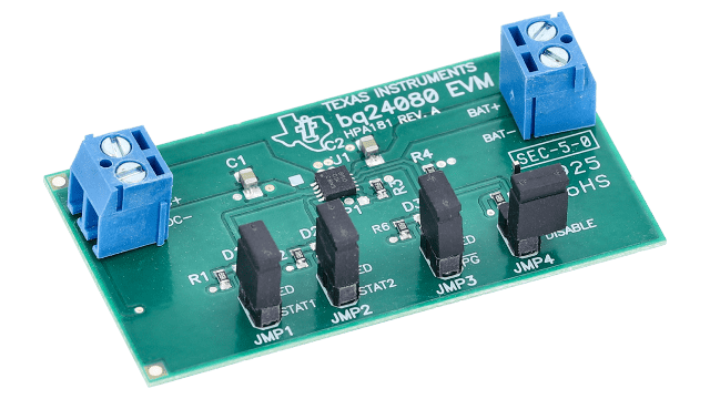
| Distributor | SKU | Stock | MOQ | 1 | 10 | 50 | 100 | 1,000 | 10,000 |
|---|---|---|---|---|---|---|---|---|---|
| DigiKey | 296-20734-ND | 4 | 1 | $58.80 | $58.80 | $58.80 | $58.80 | $58.80 | $58.80 |
| Arrow North American Components | BQ24080EVM | 0 | 1 | $56.54 | $50.66 | $50.66 | $50.24 | $50.00 | $50.00 |
| AVNET Express | BQ24080EVM | 0 | 1 | $59.78 | $59.78 | $59.78 | $59.78 | $59.78 | $59.78 |
| element14 APAC | BQ24080EVM | 0 | 1 | * $61.09 | * $61.09 | * $61.09 | * $61.09 | * $61.09 | * $61.09 |
| Farnell | BQ24080EVM | 0 | 1 | * $57.51 | * $57.51 | * $57.51 | * $57.51 | * $57.51 | * $57.51 |
| Mouser Electronics | 595-BQ24080EVM | 1 | 1 | $63.71 | $63.71 | $63.71 | $63.71 | $63.71 | $63.71 |
| Texas Instruments | BQ24080EVM | 26 | 1 | $49.00 | $49.00 | $49.00 | $49.00 | $49.00 | $49.00 |
| Verical Marketplace | BQ24080EVM | 12 | 1 | $55.35 | $55.35 | $55.35 | $55.35 | $55.35 | $55.35 |
Low-Voltage Synchronous Buck Controller with Precision Enable and No External Compensation
Texas Instruments
Low-Voltage Synchronous Buck Controller with Precision Enable and No External Compensation
| Distributor | SKU | Stock | MOQ | 1 | 10 | 50 | 100 | 1,000 | 10,000 |
|---|---|---|---|---|---|---|---|---|---|
| DigiKey | LM1771EVAL-ND | 0 | 1 | $61.25 | $61.25 | $61.25 | $61.25 | $61.25 | $61.25 |
| Arrow North American Components | LM1771EVAL | 0 | 1 | $66.65 | $65.99 | $64.68 | $64.03 | $62.13 | $61.51 |
| AVNET Express | LM1771EVAL | 0 | 1 | $59.78 | $59.78 | $59.78 | $59.78 | $59.78 | $59.78 |
| Mouser Electronics | 926-LM1771EVAL | 0 | 1 | ||||||
| Newark | LM1771EVAL | 5 | 1 | $50.73 | $50.73 | $50.73 | $50.73 | $50.73 | $50.73 |
| Texas Instruments | LM1771EVAL | 14 | 1 | $49.00 | $49.00 | $49.00 | $49.00 | $49.00 | $49.00 |
| Verical Marketplace | LM1771EVAL | 14 | 1 | $71.01 | $67.12 | $67.12 | $67.12 | $67.12 | $67.12 |
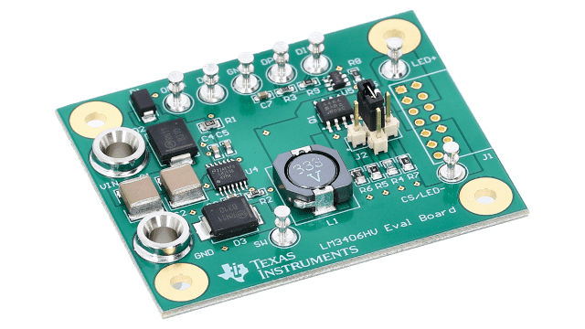
LM3406 - 1.5A High Voltage; Constant Current Buck Regulator for Driving High Current LEDs EVM
Texas Instruments
LM3406 - 1.5A High Voltage; Constant Current Buck Regulator for Driving High Current LEDs EVM
| Distributor | SKU | Stock | MOQ | 1 | 10 | 50 | 100 | 1,000 | 10,000 |
|---|---|---|---|---|---|---|---|---|---|
| DigiKey | LM3406HVEVAL/NOPB-ND | 1 | 1 | $90.00 | $90.00 | $90.00 | $90.00 | $90.00 | $90.00 |
| Mouser Electronics | N/A | 0 |
WEBENCH? Sensor Designer Photodetector Sensor Version 1 PCB (unpopulated)
Texas Instruments
WEBENCH? Sensor Designer Photodetector Sensor Version 1 PCB (unpopulated)
| Distributor | SKU | Stock | MOQ | 1 | 10 | 50 | 100 | 1,000 | 10,000 |
|---|---|---|---|---|---|---|---|---|---|
| DigiKey | SP1202S03RB-PCB/NOPB-ND | 0 | 1 | $24.00 | $24.00 | $24.00 | $24.00 | $24.00 | $24.00 |
| Distributor | SKU | Stock | MOQ | 1 | 10 | 50 | 100 | 1,000 | 10,000 |
|---|---|---|---|---|---|---|---|---|---|
| DigiKey | 296-52473-ND | 0 | $0.00 | $0.00 | $0.00 | $0.00 | $0.00 | $0.00 | |
| Arrow North American Components | TPS2061EVM-292 | 0 | 1 | $0.00 | $50.81 | $50.81 | $50.38 | $47.66 | $47.66 |
| AVNET Express | TPS2061EVM-292 | 0 | 1 | $0.00 | $0.00 | $0.00 | $0.00 | $0.00 | $0.00 |
| element14 APAC | TPS2061EVM-292 | 0 | 1 | * $61.09 | * $61.09 | * $61.09 | * $61.09 | * $61.09 | * $61.09 |
| Farnell | TPS2061EVM-292 | 0 | 1 | * $57.51 | * $57.51 | * $57.51 | * $57.51 | * $57.51 | * $57.51 |
| Mouser Electronics | 595-TPS2061EVM-292 | 0 | 1 | $0.00 | |||||
| Texas Instruments | TPS2061EVM-292 | 28 | 1 | $49.00 | $49.00 | $49.00 | $49.00 | $49.00 | $49.00 |
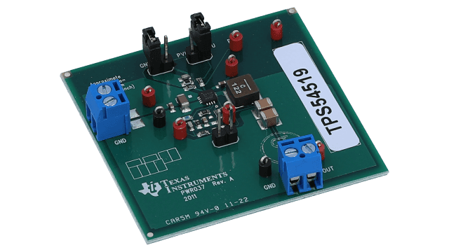
Evaluation Module for TPS54519 Synchronous Step-Down Converter
Texas Instruments
Evaluation Module for TPS54519 Synchronous Step-Down Converter
| Distributor | SKU | Stock | MOQ | 1 | 10 | 50 | 100 | 1,000 | 10,000 |
|---|---|---|---|---|---|---|---|---|---|
| DigiKey | 296-31204-ND | 3 | 1 | $58.80 | $58.80 | $58.80 | $58.80 | $58.80 | $58.80 |
| Arrow North American Components | TPS54519EVM-037 | 0 | 1 | $66.76 | $66.09 | $0.00 | $64.13 | $62.23 | $0.00 |
| AVNET Europe | TPS54519EVM-037 | 2 | 1 | * $38.90 | * $36.94 | * $33.49 | * $31.99 | * $31.99 | * $31.99 |
| AVNET Express | TPS54519EVM-037 | 0 | 1 | $30.50 | $30.50 | $30.50 | $30.50 | $30.50 | $30.50 |
| element14 APAC | TPS54519EVM-037 | 0 | 1 | * $31.17 | * $31.17 | * $31.17 | * $31.17 | * $31.17 | * $31.17 |
| Farnell | TPS54519EVM-037 | 0 | 1 | * $29.34 | * $29.34 | * $29.34 | * $29.34 | * $29.34 | * $29.34 |
| Mouser Electronics | 595-TPS54519EVM-037 | 0 | 1 | $63.71 | $63.71 | $63.71 | $63.71 | $63.71 | $63.71 |
| Newark | TPS54519EVM-037 | 0 | 1 | $25.89 | $25.89 | $25.89 | $25.89 | $25.89 | $25.89 |
| Texas Instruments | TPS54519EVM-037 | 10 | 1 | $49.00 | $49.00 | $49.00 | $49.00 | $49.00 | $49.00 |
Evaluation Module for UCC28250 Advanced PWM Controller on Primary Side Control
Texas Instruments
Evaluation Module for UCC28250 Advanced PWM Controller on Primary Side Control
| Distributor | SKU | Stock | MOQ | 1 | 10 | 50 | 100 | 1,000 | 10,000 |
|---|---|---|---|---|---|---|---|---|---|
| DigiKey | 296-31341-ND | 2 | 1 | $118.80 | $118.80 | $118.80 | $118.80 | $118.80 | $118.80 |
| Arrow North American Components | UCC28250EVM-501 | 0 | 1 | $134.69 | $133.34 | $130.69 | $129.38 | $125.54 | $124.28 |
| AVNET Express | UCC28250EVM-501 | 0 | 1 | $120.78 | $120.78 | $120.78 | $120.78 | $120.78 | $120.78 |
| Farnell | UCC28250EVM-501 | 1 | $1.00 | ||||||
| Mouser Electronics | 595-UCC28250EVM-501 | 1 | 1 | $128.71 | $128.71 | $128.71 | $128.71 | $128.71 | $128.71 |
| Newark | UCC28250EVM-501 | 0 | 1 | $102.50 | $102.50 | $102.50 | $102.50 | $102.50 | $102.50 |
| Texas Instruments | UCC28250EVM-501 | 18 | 1 | $99.00 | $99.00 | $99.00 | $99.00 | $99.00 | $99.00 |
| Verical Marketplace | UCC28250EVM-501 | 46 | 1 | $102.50 | $102.50 | $102.50 | $102.50 | $102.50 | $102.50 |
| Distributor | SKU | Stock | MOQ | 1 | 10 | 50 | 100 | 1,000 | 10,000 |
|---|---|---|---|---|---|---|---|---|---|
| DigiKey | 296-18381-ND | 0 | $0.00 | $0.00 | $0.00 | $0.00 | $0.00 | $0.00 | |
| Ameya360 | ADS8383EVM | 1 | $0.00 | $0.00 | $0.00 | $0.00 | $0.00 | $0.00 | |
| AVNET Express | ADS8383EVM | 0 | 1 | $0.00 | $0.00 | $0.00 | $0.00 | $0.00 | $0.00 |
| Mouser Electronics | 595-ADS8383EVM | 0 | 1 | ||||||
| Texas Instruments | ADS8383EVM | 16 | $99.00 | ||||||
| Utsource | ADS8383EVM | 33951 | $0.00 | $0.00 | $0.00 | $248.57 | $0.00 | $0.00 |
12-Bit, Dual 1.6 GSPS or Single 3.2 GSPS A/D Converter Reference Board
Texas Instruments
12-Bit, Dual 1.6 GSPS or Single 3.2 GSPS A/D Converter Reference Board
| Distributor | SKU | Stock | MOQ | 1 | 10 | 50 | 100 | 1,000 | 10,000 |
|---|---|---|---|---|---|---|---|---|---|
| DigiKey | 296-35879-ND | 0 | 1 | $2,998.80 | $2,998.80 | $2,998.80 | $2,998.80 | $2,998.80 | $2,998.80 |
| Mouser Electronics | N/A | 0 |
EVM430-F6779 - 3 Phase Electronic Watt-Hour EVM for Metering
Texas Instruments
EVM430-F6779 - 3 Phase Electronic Watt-Hour EVM for Metering
| Distributor | SKU | Stock | MOQ | 1 | 10 | 50 | 100 | 1,000 | 10,000 |
|---|---|---|---|---|---|---|---|---|---|
| DigiKey | 296-37565-ND | 0 | 1 | ||||||
| Arrow North American Components | EVM430-F6779 | 0 | 1 | $343.11 | $328.69 | $328.69 | $321.70 | $318.90 | $318.90 |
| AVNET Europe | EVM430-F6779 | 0 | 1 | * $446.12 | * $428.28 | * $392.59 | * $379.20 | * $379.20 | * $379.20 |
| AVNET Express | EVM430-F6779 | 0 | 1 | $364.78 | $364.78 | $364.78 | $364.78 | $364.78 | $364.78 |
| element14 APAC | EVM430-F6779 | 1 | 1 | * $403.07 | * $403.07 | * $403.07 | * $403.07 | * $403.07 | * $403.07 |
| Farnell | EVM430-F6779 | 1 | 1 | * $407.54 | * $407.54 | * $407.54 | * $407.54 | * $407.54 | * $407.54 |
| Mouser Electronics | 595-EVM430-F6779 | 3 | 1 | $365.76 | $365.76 | $365.76 | $365.76 | $365.76 | $365.76 |
| Newark | EVM430-F6779 | 0 | 1 | $420.75 | $412.50 | $412.50 | $412.50 | $412.50 | $412.50 |
| Texas Instruments | EVM430-F6779 | 13 | 1 | $275.00 | $275.00 | $275.00 | $275.00 | $275.00 | $275.00 |
| Verical Marketplace | EVM430-F6779 | 47 | 1 | $392.86 | $371.62 | $366.67 | $366.67 | $366.67 | $366.67 |
| Win Source | EVM430-F6779 | 1 | 1 |