
AD9171-FMC-EBZ
Analog Devices Inc.
The AD9171 is a high performance, dual, 16-bit digital-to-analog converter (DAC) that supports DAC sample rates to 6.2 GSPS. The device features an 8-lane, 15.4 Gbps JESD204B data input port, a high performance, on-chip DAC clock multiplier, and digital signal processing capabilities targeted at single-band direct to radio frequency (RF) wireless applications.The AD9171 features one complex data input channels per RF DAC. Each data input channel includes a configurable gain stage, an interpolation filter, and a channel numerically controlled oscillator (NCO) for flexible, frequency planning. The device supports up to a 516 MSPS complex data rate per input channel.The AD9171 is available in a 144-ball BGA_ED package.PRODUCT HIGHLIGHTS Supports one complex data input channel per RF DAC at a maximum complex input data rate of 513 MSPS with 12-bitresolution and 516 MSPS with 16-bit resolution options. There is one independent NCO per input channel. Low power dual converter decreases the amount of power consumption needed in high bandwidth and multichannel applications.?APPLICATIONS Wireless communications infrastructure Single-band base station radios Instrumentation, automatic test equipment (ATE)
| Distributor | SKU | Stock | MOQ | 1 | 10 | 50 | 100 | 1,000 | 10,000 |
|---|---|---|---|---|---|---|---|---|---|
| DigiKey | AD9171-FMC-EBZ-ND | 1 | 1 | $1,762.26 | $1,762.26 | $1,762.26 | $1,762.26 | $1,762.26 | $1,762.26 |
| Analog Devices Inc | AD9171-FMC-EBZ | 0 | $1,391.92 | $1,391.92 | $1,391.92 | $1,391.92 | $1,391.92 | $1,391.92 | |
| Arrow North American Components | AD9171-FMC-EBZ | 0 | 1 | $1,443.98 | $1,429.54 | $1,401.09 | $1,387.08 | $1,345.88 | $1,332.43 |
| Mouser Electronics | 584-9171FMCEBZ | 2 | 1 | $1,508.00 | $1,508.00 | $1,508.00 | $1,508.00 | $1,508.00 | $1,508.00 |
| Verical Marketplace | AD9171-FMC-EBZ | 7 | 1 | $1,434.67 | $1,434.67 | $1,434.67 | $1,434.67 | $1,434.67 | $1,434.67 |

AD9208-DUAL-EBZ
Analog Devices Inc.
The AD9208 is a dual, 14-bit, 3 GSPS analog-to-digital converter (ADC). The device has an on-chip buffer and a sample-and-hold circuit designed for low power, small size, and ease of use. This product is designed to support communications applications capable of direct sampling wide bandwidth analog signals of up to 5 GHz. The ?3 dB bandwidth of the ADC input is 9 GHz. The AD9208 is optimized for wide input bandwidth, high sampling rate, excellent linearity, and low power in a small package.The dual ADC cores feature a multistage, differential pipelined architecture with integrated output error correction logic. Each ADC features wide bandwidth inputs supporting a variety of user-selectable input ranges. An integrated voltage referenceeases design considerations. The analog input and clock signals are differential inputs. The ADC data outputs are internally connected to four digital downconverters (DDCs) through a crossbar mux. Each DDC consists of up to five cascaded signalprocessing stages: a 48-bit frequency translator (numerically controlled oscillator (NCO)), and up to four half-band decimationfilters. The NCO has the option to select preset bands over the general-purpose input/output (GPIO) pins, which enables the selection of up to three bands. Operation of the AD9208 between the DDC modes is selectable via SPI-programmable profiles.In addition to the DDC blocks, the AD9208 has several functions that simplify the automatic gain control (AGC) function in acommunications receiver. The programmable threshold detector allows monitoring of the incoming signal power using the fast detect control bits in Register 0x0245 of the ADC. If the input signal level exceeds the programmable threshold, the fast detect indicator goes high. Because this threshold indicator has low latency, the user can quickly turn down the system gain to avoidan overrange condition at the ADC input. In addition to the fast detect outputs, the AD9208 also offers signal monitoring capability. The signal monitoring block provides additional information about the signal being digitized by the ADC.The user can configure the Subclasss 1 JESD204B-based high speed serialized output in a variety of one-lane, two-lane, four-lane, and eight-lane configurations, depending on the DDC configuration and the acceptable lane rate of the receiving logic device. Multidevice synchronization is supported through the SYSREF? and SYNCINB? input pins.The AD9208 has flexible power-down options that allow significant power savings when desired. All of these features canbe programmed using a 3-wire serial port interface (SPI).The AD9208 is available in a Pb-free, 196-ball BGA, specified over the ?40?C to +85?C ambient temperature range. Thisproduct is protected by a U.S. patent.Note that throughout this data sheet, multifunction pins, such as FD_A/GPIO_A0, are referred to either by the entire pin name or by a single function of the pin, for example, FD_A, when only that function is relevant.Product Highlights Wide, input ?3 dB bandwidth of 9 GHz supports direct radio frequency (RF) sampling of signals up to about 5 GHz. Four integrated, wideband decimation filter and NCO blocks supporting multiband receivers. Fast NCO switching enabled through GPIO pins. A SPI controls various product features and functions to meet specific system requirements. Programmable fast overrange detection and signal monitoring. On-chip temperature dioide for system thermal management. 12mm ? 12mm 196-Lead BGAApplications Diversity multiband, multimode digital receivers 3G/4G, TD-SCDMA, W-CDMA, GSM, LTE, LTE-A Electronic test and measurement systems Phased array radar and electronic warfare DOCSIS 3.0 CMTS upstream receive paths HFC digital reverse path receivers
| Distributor | SKU | Stock | MOQ | 1 | 10 | 50 | 100 | 1,000 | 10,000 |
|---|---|---|---|---|---|---|---|---|---|
| DigiKey | 505-AD9208-DUAL-EBZ-ND | 4 | 1 | $3,189.89 | $3,189.89 | $3,189.89 | $3,189.89 | $3,189.89 | $3,189.89 |
| Analog Devices Inc | AD9208-DUAL-EBZ | 0 | $3,044.42 | $3,044.42 | $3,044.42 | $3,044.42 | $3,044.42 | $3,044.42 | |
| Arrow North American Components | AD9208-DUAL-EBZ | 0 | 1 | $3,014.28 | $2,984.14 | $2,924.75 | $2,895.51 | $2,809.51 | $2,781.41 |
| element14 APAC | AD9208-DUAL-EBZ | 2 | 1 | * $3,346.02 | * $3,346.02 | * $3,346.02 | * $3,346.02 | * $3,346.02 | * $3,346.02 |
| Farnell | AD9208-DUAL-EBZ | 2 | 1 | * $3,183.45 | * $3,183.45 | * $3,183.45 | * $3,183.45 | * $3,183.45 | * $3,183.45 |
| Mouser Electronics | 584-AD9208-DUAL-EBZ | 3 | 1 | $3,348.26 | $3,348.26 | $3,348.26 | $3,348.26 | $3,348.26 | $3,348.26 |
| Newark | AD9208-DUAL-EBZ | 2 | 1 | $3,190.01 | $3,190.01 | $3,190.01 | $3,190.01 | $3,190.01 | $3,190.01 |
| Verical Marketplace | AD9208-DUAL-EBZ | 9 | 1 | $3,137.93 | $3,137.93 | $3,137.93 | $3,137.93 | $3,137.93 | $3,137.93 |

AD9212-65EBZ
Analog Devices Inc.
The AD9212 is an octal, 10-bit, 40 MSPS/65 MSPS ADC with an on-chip sample-and-hold circuit designed for low cost, low power,small size, and ease of use. Operating at a conversion rate of up to 65 MSPS, it is optimized for outstanding dynamic performance and low power in applications where a small package size is critical.The ADC requires a single 1.8 V power supply and LVPECL-/ CMOS-/LVDS-compatible sample rate clock for full performanceoperation. No external reference or driver components arerequired for many applications.The ADC automatically multiplies the sample rate clock forthe appropriate LVDS serial data rate. A data clock (DCO)for capturing data on the output and a frame clock (FCO) for signaling a new output byte are provided. Individual channelpower-down is supported and typically consumes less than 2 mW when all channels are disabled.The ADC contains several features designed to maximizeflexibility and minimize system cost, such as programmableclock and data alignment and programmable digital test patterngeneration. The available digital test patterns include built-in deterministic and pseudorandom patterns, along with custom user-defined test patterns entered via the serial port interface (SPI).The AD9212 is available in a RoHS-compliant, 64-lead LFCSP. It isspecified over the industrial temperature range of ?40?C to +85?C.PRODUCT HIGHLIGHTS Small Footprint. Eight ADCs are contained in a small package. Low Power of 100 mW per Channel at 65 MSPS. Ease of Use. A data clock output (DCO) operates up to 300 MHz and supports double data rate (DDR) operation. User Flexibility. SPI control offers a wide range of flexible features to meet specific system requirements. Pin-Compatible Family. This includes the AD9222 (12-bit) and AD9252 (14-bit).APPLICATIONS Medical imaging and nondestructive ultrasound Portable ultrasound and digital beam-forming systems Quadrature radio receivers Diversity radio receivers Tape drives Optical networking Test equipment
| Distributor | SKU | Stock | MOQ | 1 | 10 | 50 | 100 | 1,000 | 10,000 |
|---|---|---|---|---|---|---|---|---|---|
| DigiKey | AD9212-65EBZ-ND | 0 | 1 | $378.41 | $378.41 | $378.41 | $378.41 | $378.41 | $378.41 |
| Analog Devices Inc | AD9212-65EBZ | 0 | $345.19 | $345.19 | $345.19 | $345.19 | $345.19 | $345.19 | |
| Arrow North American Components | AD9212-65EBZ | 0 | 1 | $370.43 | $366.73 | $359.43 | $355.84 | $345.27 | $341.81 |
| Mouser Electronics | 584-AD9212-65EBZ | 0 | 1 | $293.55 | $293.55 | $293.55 | $293.55 | $293.55 | $293.55 |
| Verical Marketplace | AD9212-65EBZ | 11 | 1 | $385.63 | $385.63 | $385.63 | $385.63 | $385.63 | $385.63 |
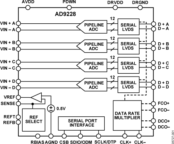
AD9228-65EBZ
Analog Devices Inc.
The AD9228 is a quad, 12-bit, 40/65 MSPS analog-to-digital converter (ADC) with an on-chip sample-and-hold circuit designed for low cost, low power, small size, and ease of use. The product operates at a conversion rate of up to 65 MSPS and is optimized for outstanding dynamic performance and low power in applications where a small package size is critical. The ADC requires a single 1.8 V power supply and LVPECL-/ CMOS-/LVDS-compatible sample rate clock for full performance operation. No external reference or driver components are required for many applications. The ADC automatically multiplies the sample rate clock for the appropriate LVDS serial data rate. A data clock output (DCO) for capturing data on the output and a frame clock output (FCO) for signaling a new output byte are provided. Individual channel power-down is supported and typically consumes The ADC contains several features designed to maximize flexibility and minimize system cost, such as programmable clock and data alignment and programmable digital test pattern generation. The available digital test patterns include built-in deterministic and pseudorandom patterns, along with custom user-defined test patterns entered via the serial port interface (SPI). The AD9228 is available in an RoHS compliant, 48-lead LFCSP. It is specified over the industrial temperature range of ?40?C to +85?C.PRODUCT HIGHLIGHTSSmall Footprint. Four ADCs are contained in a small, space-saving package. Low power of 119 mW/channel at 65 MSPS. Ease of Use. A data clock output (DCO) is provided that operates at frequencies of up to 390 MHz and supports double data rate (DDR) operation.User Flexibility. The SPI control offers a wide range of flexible features to meet specific system requirements. Pin-Compatible Family. This includes the AD9287 (8-bit), AD9219 (10-bit), and AD9259 (14-bit).?APPLICATIONSMedical imaging and nondestructive ultrasound Portable ultrasound and digital beam-forming systemsQuadrature radio receivers Diversity radio receivers Tape drives Optical networking Test equipment
| Distributor | SKU | Stock | MOQ | 1 | 10 | 50 | 100 | 1,000 | 10,000 |
|---|---|---|---|---|---|---|---|---|---|
| DigiKey | AD9228-65EBZ-ND | 0 | 1 | $283.08 | $283.08 | $283.08 | $283.08 | $283.08 | $283.08 |
| Analog Devices Inc | AD9228-65EBZ | 0 | $263.76 | $263.76 | $263.76 | $263.76 | $263.76 | $263.76 | |
| Arrow Europe | AD9228-65EBZ | 1 | 1 | $218.36 | $218.36 | $218.36 | $218.36 | $218.36 | $218.36 |
| Arrow North American Components | AD9228-65EBZ | 0 | 1 | $274.92 | $272.17 | $266.75 | $264.09 | $256.24 | $253.68 |
| element14 APAC | AD9228-65EBZ | 0 | 1 | * $279.06 | * $279.06 | * $279.06 | * $279.06 | * $279.06 | * $279.06 |
| Farnell | AD9228-65EBZ | 0 | 1 | * $233.98 | * $233.98 | * $233.98 | * $233.98 | * $233.98 | * $233.98 |
| Mouser Electronics | 584-AD9228-65EBZ | 3 | 1 | $272.97 | $272.97 | $272.97 | $272.97 | $272.97 | $272.97 |
| Verical Marketplace | AD9228-65EBZ | 14 | 1 | $286.20 | $286.20 | $286.20 | $286.20 | $286.20 | $286.20 |

AD9230-250EBZ
Analog Devices Inc.
The AD9230 is a 12-bit monolithic sampling analog-to-digital converter optimized for high performance, low power, and ease of use. The product operates at up to a 250 MSPS conversion rate and is optimized for outstanding dynamic performance in wideband carrier and broadband systems. All necessary functions, including a track-and-hold (T/H) and voltage reference, are included on the chip to provide a complete signal conversion solution. The ADC requires a 1.8 V analog voltage supply and a differential clock for full performance operation. The digital outputs are LVDS (ANSI-644) compatible and support either twos complement, offset binary format, or Gray code. A data clock output is available for proper output data timing.Fabricated on an advanced CMOS process, the AD9230 is available in a 56-lead LFCSP, specified over the industrial temperature range (?40?C to +85?C).PRODUCT HIGHLIGHTS High Performance?Maintains 64.9 dBFS SNR @ 250 MSPS with a 70 MHz input. Low Power?Consumes only 434 mW @ 250 MSPS. Ease of Use?LVDS output data and output clock signal allow interface to current FPGA technology. The on-chip reference and sample and hold provide flexibility in system design. Use of a single 1.8 V supply simplifies system power supply design. Serial Port Control?Standard serial port interface supports various product functions, such as data formatting, disabling the clock duty cycle stabilizer, power-down, gain adjust, and output test pattern generation. Pin-Compatible Family?10-bit pin-compatible family offered as AD9211.APPLICATIONS Wireless and wired broadband communications Cable reverse path Communications test equipment Radar and satellite subsystems Power amplifier linearization
| Distributor | SKU | Stock | MOQ | 1 | 10 | 50 | 100 | 1,000 | 10,000 |
|---|---|---|---|---|---|---|---|---|---|
| DigiKey | AD9230-250EBZ-ND | 0 | 1 | $283.08 | $283.08 | $283.08 | $283.08 | $283.08 | $283.08 |
| Analog Devices Inc | AD9230-250EBZ | 0 | $263.76 | $263.76 | $263.76 | $263.76 | $263.76 | $263.76 | |
| Arrow North American Components | AD9230-250EBZ | 0 | 1 | $274.92 | $272.17 | $266.75 | $264.09 | $256.24 | $253.68 |
| Verical Marketplace | AD9230-250EBZ | 24 | 1 | $286.20 | $286.20 | $286.20 | $286.20 | $286.20 | $286.20 |

AD9234-1000EBZ
Analog Devices Inc.
The AD9234 is a dual, 12-bit, 1 GSPS/500 MSPS ADC. The device has an on-chip buffer and sample-and-hold circuit designed for low power, small size, and ease of use. This product is designed for sampling wide bandwidth analog signals. The AD9234 is optimized for wide input bandwidth, high sampling rate, excellent linearity, and low power in a small package.The dual ADC cores feature a multistage, differential pipelined architecture with integrated output error correction logic. Each ADC features wide bandwidth buffered inputs supporting a variety of user-selectable input ranges. An integrated voltage reference eases design considerations. Each ADC data output is internally connected to an optional decimate-by-2 block. The AD9234 has several functions that simplify the automatic gain control (AGC) function in a communications receiver.?The programmable threshold detector allows monitoring of the incoming signal power using the fast detect output bits of the ADC. If the input signal level exceeds the programmable threshold, the fast detect indicator goes high. Because this threshold indicator has low latency, the user can quickly turn down the system gain to avoid an overrange condition at the ADC input. In addition to the fast detect outputs, the AD9234 also offers signal monitoring capability. The signal monitoring block provides additional information about the signal being digitized by the ADC.Users can configure the Subclass 1 JESD204B-based high speed serialized output in a variety of one-, two-, or four-lane configurations, depending on the acceptable lane rate of the receiving logic device and the sampling rate of the ADC. Multiple device synchronization is supported through the SYSREF? and SYNCINB? input pins.The AD9234 has flexible power-down options that allow significant power savings when desired. All of these features can be programmed using a 1.8 V to 3.3 V capable 3-wire SPI.The AD9234 is available in a Pb-free, 64-lead LFCSP and is specified over the ?40?C to +85?C industrial temperature range. This product is protected by a U.S. patent.Product Highlights Low power consumption analog core, 12-bit, 1.0 GSPS dual analog-to-digital converter (ADC) with 1.5 W per channel. Wide full power bandwidth supports IF sampling of signals up to 2 GHz. Buffered inputs with programmable input termination eases filter design and implementation. Flexible serial port interface (SPI) controls various product features and functions to meet specific system requirements. Programmable fast overrange detection. 9 mm ? 9 mm 64-lead LFCSP. Pin compatible with the AD9680 14-bit, 1 GSPS dual ADC.Applications Communications Diversity multiband, multimode digital receivers 3G/4G, TD-SCDMA, W-CDMA, GSM, LTE Point-to-point radio systems Digital predistortion observation path General-purpose software radios Ultrawideband satellite receiver Instrumentation (spectrum analyzers, network analyzers, integrated RF test solutions) Digital oscilloscopes High speed data acquisition systems DOCSIS 3.0 CMTS upstream receive paths HFC digital reverse path receivers
| Distributor | SKU | Stock | MOQ | 1 | 10 | 50 | 100 | 1,000 | 10,000 |
|---|---|---|---|---|---|---|---|---|---|
| DigiKey | AD9234-1000EBZ-ND | 1 | 1 | $1,192.04 | $1,192.04 | $1,192.04 | $1,192.04 | $1,192.04 | $1,192.04 |
| Analog Devices Inc | AD9234-1000EBZ | 0 | $1,099.78 | $1,099.78 | $1,099.78 | $1,099.78 | $1,099.78 | $1,099.78 | |
| Arrow North American Components | AD9234-1000EBZ | 0 | 1 | $1,180.24 | $1,168.44 | $1,145.19 | $1,133.74 | $1,100.06 | $1,089.06 |
| Mouser Electronics | 584-AD9234-1000EBZ | 0 | 1 | $1,020.28 | $1,020.28 | $1,020.28 | $1,020.28 | $1,020.28 | $1,020.28 |
| Newark | AD9234-1000EBZ | 0 | $973.32 | $973.32 | $973.32 | $973.32 | $973.32 | $973.32 | |
| Verical Marketplace | AD9234-1000EBZ | 7 | 1 | $1,228.66 | $1,228.66 | $1,228.66 | $1,228.66 | $1,228.66 | $1,228.66 |

AD9265-FMC-125EBZ
Analog Devices Inc.
The AD9265 is a 16-bit, 125 MSPS analog-to-digital converter (ADC). The AD9265 is designed to support communications applications where high performance combined with low cost, small size, and versatility is desired.The ADC core features a multistage, differential pipelined architecture with integrated output error correction logic to provide 16-bit accuracy at 125 MSPS data rates and guarantees no missing codes over the full operating temperature range.The ADC features a wide bandwidth differential sample-and-hold analog input amplifier supporting a variety of user-selectable input ranges. It is suitable for multiplexed systems that switch full-scale voltage levels in successive channels and for sampling single-channel inputs at frequencies well beyond the Nyquist rate.Combined with power and cost savings over previously available ADCs, the AD9265 is suitable for applications in communications, instrumentation and medical imaging. A differential clock input controls all internal conversion cycles. A duty cycle stabilizer provides the means to compensate for variations in the ADC clock duty cycle, allowing the converters to maintain excellent performance over a wide range of input clock duty cycles. An integrated voltage reference eases design considerations.The ADC output data format is either parallel 1.8 V CMOS or LVDS (DDR). A data output clock is provided to ensure proper latch timing with receiving logic.Programming for setup and control is accomplished using a 3-wire SPI-compatible serial interface. Flexible power-down options allow significant power savings, when desired. An optional on-chip dither function is available to improve SFDR performance with low power analog input signals.The AD9265 is available in a Pb-free, 48-lead LFCSP and is specified over the industrial temperature range of ?40?C to +85?C.APPLICATIONS Communications Multimode digital receivers (3G) GSM, EDGE, W-CDMA, LTE, CDMA2000, WiMAX, and TD-SCDMA Smart antenna systems General-purpose software radios Broadband data applications Ultrasound equipmentPRODUCT HIGHLIGHTS On-chip dither option for improved SFDR performance with low power analog input. Proprietary differential input that maintains excellent SNR performance for input frequencies up to 300 MHz. Operation from a single 1.8 V supply and a separate digital output driver supply accommodating 1.8 V CMOS or LVDS outputs. Standard serial port interface (SPI) that supports various product features and functions, such as data formatting (offset binary, twos complement, or gray coding), enabling the clock duty cycle stabilizer, DCS, power-down, test modes, and voltage reference mode. Pin compatibility with the AD9255, allowing a simple migration from 16 bits down to 14 bits.
| Distributor | SKU | Stock | MOQ | 1 | 10 | 50 | 100 | 1,000 | 10,000 |
|---|---|---|---|---|---|---|---|---|---|
| DigiKey | AD9265-FMC-125EBZ-ND | 0 | 1 | $431.15 | $431.15 | $431.15 | $431.15 | $431.15 | $431.15 |
| Mouser Electronics | 584-AD9265-FMC125EBZ | 0 | 1 | ||||||
| Win Source | AD9265-FMC-125EBZ | 1 | 1 |

AD9278-50EBZ
Analog Devices Inc.
The AD9278 is designed for low cost, low power, small size,and ease of use. It contains eight channels of a variable gain amplifier (VGA) with a low noise preamplifier (LNA); an anti-aliasing filter (AAF); a 12-bit, 10 MSPS to 65 MSPS analog-to-digital converter (ADC); and an I/Q demodulator with programmable phase rotation.Each channel features a variable gain range of 45 dB, a fully differential signal path, an active input preamplifier termination, a maximum gain of up to 51 dB, and an ADC with a conversion rate of up to 65 MSPS. The channel is optimized for dynamic performance and low power in applications where a small package size is critical.The LNA has a single-ended-to-differential gain that is selectable through the SPI. The LNA input noise is typically 1.3 nV/?Hz at a gain of 21.3 dB, and the combined input-referred noise of the entire channel is 1.3 nV/?Hz at maximum gain. Assuming a 15 MHz noise bandwidth (NBW) and a 21.3 dB LNA gain, the input SNR is roughly 88 dB. In CW Doppler mode, each LNA output drives an I/Q demodulator. Each demodulator has independently programmable phase rotation through the SPI with 16 phase settings.The AD9278 requires a LVPECL-/CMOS-/LVDS-compatible sample rate clock for full performance operation. No external reference or driver components are required for many applications.The ADC automatically multiplies the sample rate clock forthe appropriate LVDS serial data rate. A data clock (DCO?) for capturing data on the output and a frame clock (FCO?) trigger for signaling a new output byte are provided.Powering down individual channels is supported to increase battery life for portable applications. A standby mode option allows quick power-up for power cycling. In CW Doppler operation, the VGA, AAF, and ADC are powered down. The power of the TGC path scales with selectable ADC speed power modes.The ADC contains several features designed to maximize flexibility and minimize system cost, such as a programmable clock, data alignment, and programmable digital test pattern generation. The digital test patterns include built-in fixed patterns, built-in pseudo-random patterns, and custom user-defined test patterns entered via the serial port interface.Fabricated in an advanced BiCMOS process, the AD9278 is available in a 10 mm ? 10 mm, RoHS compliant, 144-lead BGA. It is specified over the industrial temperature rangeof ?40?C to +85?C.
| Distributor | SKU | Stock | MOQ | 1 | 10 | 50 | 100 | 1,000 | 10,000 |
|---|---|---|---|---|---|---|---|---|---|
| DigiKey | 505-AD9278-50EBZ-ND | 1 | 1 | $337.82 | $337.82 | $337.82 | $337.82 | $337.82 | $337.82 |
| Analog Devices Inc | AD9278-50EBZ | 0 | $307.20 | $307.20 | $307.20 | $307.20 | $307.20 | $307.20 | |
| Arrow North American Components | AD9278-50EBZ | 0 | 1 | $288.62 | $288.62 | $288.62 | $288.62 | $288.62 | $288.62 |
| Mouser Electronics | 584-AD9278-50EBZ | 1 | 1 | $340.98 | $340.98 | $340.98 | $340.98 | $340.98 | $340.98 |
| Newark | AD9278-50EBZ | 0 | $271.88 | $271.88 | $271.88 | $271.88 | $271.88 | $271.88 | |
| Verical Marketplace | AD9278-50EBZ | 6 | 1 | $316.64 | $316.64 | $316.64 | $316.64 | $316.64 | $316.64 |

AD9484-500EBZ
Analog Devices Inc.
The AD9484 is an 8-bit, monolithic, sampling analog-to-digital converter (ADC) optimized for high performance, low power, and ease of use. The part operates at up to a 500 MSPS conversion rate and is optimized for outstanding dynamic performance in wideband carrier and broadband systems. All necessary functions, including a sample-and-hold and voltage reference, are included on the chip to provide a complete signal conversion solution. The VREF pin can be used to monitor the internal reference or provide an external voltage reference (external reference mode must be enabled through the SPI port).The ADC requires a 1.8 V analog voltage supply and a differential clock for full performance operation. The digital outputs are LVDS (ANSI-644) compatible and support twos complement, offset binary format, or Gray code. A data clock output is available for proper output data timing.Fabricated on an advanced BiCMOS process, the AD9484 is available in a 56-lead LFCSP, and is specified over the industrial temperature range (?40?C to +85?C). This product is protected under U.S. and international patents.PRODUCT HIGHLIGHTS High Performance. Maintains 47 dBFS SNR at 500 MSPS with a 250 MHz input. Ease of Use. LVDS output data and output clock signal allow interface to current FPGA technology. The on-chip reference and sample and hold provide flexibility in system design. Use of a single 1.8 V supply simplifies system power supply design. Serial Port Control. Standard serial port interface supports various product functions, such as data formatting, disabling the clock duty cycle stabilizer, power down, gain adjust, and output test pattern generation.APPLICATIONS Wireless and wired broadband communications Cable reverse path Communications test equipment Low cost digital oscilloscopes Satellite subsystems Power amplifier linearization
| Distributor | SKU | Stock | MOQ | 1 | 10 | 50 | 100 | 1,000 | 10,000 |
|---|---|---|---|---|---|---|---|---|---|
| DigiKey | AD9484-500EBZ-ND | 1 | 1 | $337.82 | $337.82 | $337.82 | $337.82 | $337.82 | $337.82 |
| Analog Devices Inc | AD9484-500EBZ | 0 | $307.20 | $307.20 | $307.20 | $307.20 | $307.20 | $307.20 | |
| Arrow North American Components | AD9484-500EBZ | 0 | 1 | $329.68 | $326.38 | $319.89 | $316.69 | $307.28 | $304.21 |
| Mouser Electronics | 584-AD9484-500EBZ | 3 | 1 | $332.82 | $332.82 | $332.82 | $332.82 | $332.82 | $332.82 |
| Verical Marketplace | AD9484-500EBZ | 25 | 1 | $316.64 | $316.64 | $316.64 | $316.64 | $316.64 | $316.64 |

AD9514/PCBZ
Analog Devices Inc.
The AD9514 features a multi-output clock distribution IC in a design that emphasizes low jitter and phase noise to maximize data converter performance. Other applications with demanding phase noise and jitter requirements also benefit from this part.There are three independent clock outputs. Two of the outputs are LVPECL, and the third output can be set to either LVDS or CMOS levels. The LVPECL outputs operate to 1.6 GHz, and the third output operates to 800 MHz in LVDS mode and to 250 MHz in CMOS mode. Each output has a programmable divider, which can be set to divide by a selected set of integers ranging from 1 to 32. The phase of one clock output relative to another clock output can be set by means of a divider phase select function that serves as a coarse timing adjustment. The LVDS/CMOS output features a delay element with three selectable full-scale delay values (1.5 ns, 5 ns, and 10 ns), each with 16 steps of fine adjustment. The AD9514 does not require an external controller for operation or setup. The device is programmed by means of 11 pins (S0 to S10) using 4-level logic. The programming pins are internally biased to ? VS. The VREF pin provides a level of ? VS. VS (3.3 V) and GND (0 V) provide the other two logic levels. The AD9514 is ideally suited for data converter clocking applications where maximum converter performance is achieved by encode signals with subpicosecond jitter. The AD9514 is available in a 32-lead LFCSP and operates from a single 3.3 V supply. The temperature range is ?40?C to +85?C. APPLICATIONSLow jitter, low phase noise clock distribution Clocking high speed ADC, DAC, DDS, DDC, DUC, MxFEsHigh performance wireless transceiversHigh performance instrumentationBroadband infrastructureATE
| Distributor | SKU | Stock | MOQ | 1 | 10 | 50 | 100 | 1,000 | 10,000 |
|---|---|---|---|---|---|---|---|---|---|
| DigiKey | 505-AD9514/PCBZ-ND | 0 | 1 | $308.85 | $308.85 | $308.85 | $308.85 | $308.85 | $308.85 |
| Analog Devices Inc | AD9514/PCBZ | 0 | $291.84 | $291.84 | $291.84 | $291.84 | $291.84 | $291.84 | |
| Arrow North American Components | AD9514/PCBZ | 0 | 1 | $300.67 | $297.66 | $291.74 | $288.82 | $280.24 | $216.66 |
| element14 APAC | AD9514/PCBZ | 2 | 1 | * $264.29 | * $264.29 | * $264.29 | * $264.29 | * $264.29 | * $264.29 |
| Farnell | AD9514/PCBZ | 0 | 1 | * $230.08 | * $230.08 | * $230.08 | * $230.08 | * $230.08 | * $230.08 |
| Mouser Electronics | 584-AD9514PCBZ | 0 | 1 | $285.65 | $285.65 | $285.65 | $285.65 | $285.65 | $285.65 |
| Verical Marketplace | AD9514/PCBZ | 12 | 1 | $313.00 | $294.86 | $290.93 | $290.93 | $290.93 | $290.93 |