|
|
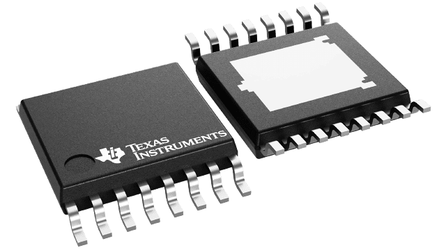
Texas Instruments
TPS2HB35CQPWPRQ1
|
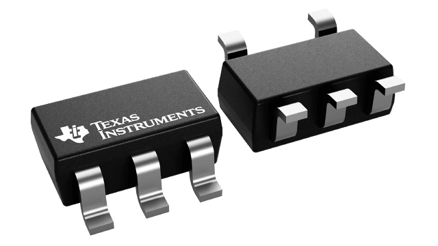
Texas Instruments
TPS3840DL45DBVR
|

Texas Instruments
TPS3840PL30DBVR
|
Texas Instruments
XPS628660AYCGR
|
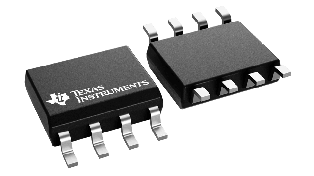
Texas Instruments
TLV9102IDSGR
|

Texas Instruments
TLV9301IDBVR
|
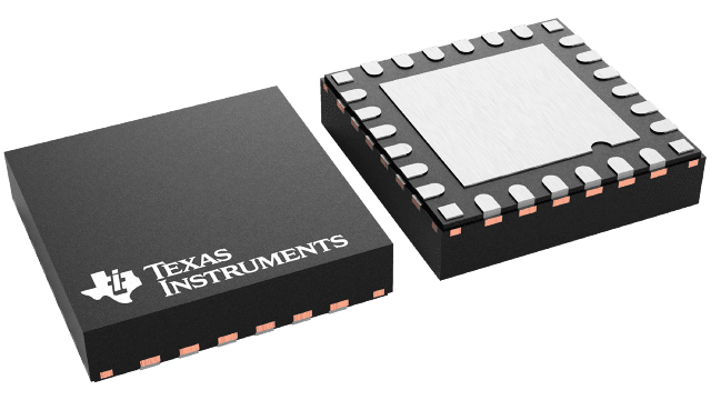
Texas Instruments
CDCE6214TWRGERQ1
|

Texas Instruments
CDCE6214TWRGETQ1
|
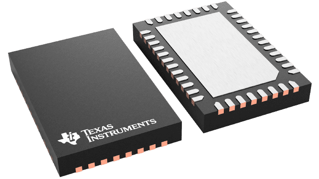
Texas Instruments
DS160PR410RNQT
|
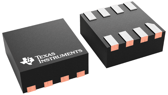
Texas Instruments
DS90LV028AQDQFTQ1
|
| Price |
|
|
|
|
|
|
|
|
|
|
|
| RoHS |
|
Not Compliant |
Y |
Y |
Y |
Y |
Y |
Y |
Y |
Y |
See ti.com |
| Lead Status |
|
Y |
Y |
Y |
Y |
Y |
Y |
Y |
Y |
Y |
See ti.com |
| Device type |
|
High-side switches |
|
|
|
|
|
|
|
Redriver |
|
| FET |
|
Internal |
|
|
|
|
|
|
|
|
|
| Approx. price(US$) |
|
.935 | 1ku |
0.40 | 1ku |
0.40 | 1ku |
0.95 | 1ku |
0.34 | 1ku |
0.20 | 1ku |
2.478 | 1ku |
2.898 | 1ku |
5.00 | 1ku |
1.04 | 1ku |
| Imax(A) |
|
3 |
|
|
|
|
|
|
|
|
|
| Current sense accuracy |
|
+/-4% @ 1A |
|
|
|
|
|
|
|
|
|
| Ron(Typ)(mOhm) |
|
35 |
|
|
|
|
|
|
|
|
|
| Driver configuration |
|
High Side |
|
|
|
|
|
|
|
|
|
| Current limit(Min)(A) |
|
2 |
|
|
|
|
|
|
|
|
|
| HBM ESD(kV) |
|
2 |
|
|
|
|
|
|
|
|
|
| Current limit type |
|
Adjustable |
|
|
|
|
|
|
|
|
|
| Features |
|
Current sense output,Current sense/monitor,Programmable current limit,Thermal shutdown,Under voltage lock out |
Manual reset |
Manual reset |
Enable,Forced PWM,I2C,Light Load Efficiency,Output Discharge,Over Current Protection,Soft Start Fixed,Synchronous Rectification,UVLO Fixed,VID Interface |
Cost Optimized,EMI Hardened,Small Size |
Cost Optimized,EMI Hardened |
Integrated EEPROM,Pin programmable,Serial interface |
Integrated EEPROM,Pin programmable,Serial interface |
|
|
| Operating voltage(Max)(V) |
|
28 |
|
|
|
|
|
|
|
|
|
| Function |
|
Adjustable current limit,Automotive load dump compatibility,Current monitoring,Inductive load compatibility,Inrush current control,Short circuit protection,Thermal shutdown |
|
|
|
|
|
Clock generator |
Clock generator |
|
Receiver |
| Operating temperature range(C) |
|
-40 to 125 |
-40 to 125 |
-40 to 125 |
-40 to 125 |
-40 to 125 |
-40 to 125 |
-40 |
-40 |
-40 to 85 |
-40 to 125 |
| Number of channels(#) |
|
2 |
|
|
|
2 |
1 |
|
|
4 |
|
| Operating voltage(Min)(V) |
|
6 |
|
|
|
|
|
|
|
|
|
| Current limit accuracy |
|
+25%/-10% |
|
|
|
|
|
|
|
|
|
| Number of supplies monitored |
|
|
1 |
1 |
|
|
|
|
|
|
|
| VCC(Max)(V) |
|
|
10 |
10 |
|
|
|
|
|
|
|
| Rating |
|
|
Catalog |
Catalog |
Catalog |
Catalog |
Catalog |
Automotive |
Automotive |
Catalog |
Automotive |
| Package size |
|
|
mm2 |
mm2 |
mm2 |
mm2 |
mm2 |
|
|
|
|
| Threshold voltage 1(Typ)(V) |
|
|
Trimmable,1.8,2,2.2,2.5,2.7,2.8,2.9,3,4.3,4.5 |
Trimmable,1.8,2,2.2,2.5,2.7,2.8,2.9,3,4.3,4.5 |
|
|
|
|
|
|
|
| VCC(Min)(V) |
|
|
1.5 |
1.5 |
|
|
|
|
|
|
|
| Monitored voltage 1 (typ)(Nom)(V) |
|
|
Adjustable,2.5,3,3.3,5 |
Adjustable,2.5,3,3.3,5 |
|
|
|
|
|
|
|
| Watchdog timer WDI(sec) |
|
|
None |
None |
|
|
|
|
|
|
|
| Iq(Typ)(uA) |
|
|
0.3 |
0.3 |
|
|
|
|
|
|
|
| Output driver type/reset output |
|
|
Active-high,Active-low,Open-drain,Push-pull |
Active-high,Active-low,Open-drain,Push-pull |
|
|
|
|
|
|
|
| Package Group |
|
|
SOT-23|5 |
SOT-23|5 |
DSBGA|15 |
SOIC|8,TSSOP|8,WSON|8 |
SOT-23|5 |
|
|
WQFN|40 |
SOIC|8,WSON|8 |
| Time delay(ms) |
|
|
Programmable |
Programmable |
|
|
|
|
|
|
|
| Switching frequency(Typ)(kHz) |
|
|
|
|
2400 |
|
|
|
|
|
|
| Control mode |
|
|
|
|
DCS-Control |
|
|
|
|
|
|
| Vin(Max)(V) |
|
|
|
|
5.5 |
|
|
|
|
|
|
| Type |
|
|
|
|
Converter |
|
|
|
|
|
|
| Iout(Max)(A) |
|
|
|
|
6 |
|
|
|
|
|
|
| Vout(Max)(V) |
|
|
|
|
1.675 |
|
|
|
|
|
|
| Iq(Typ)(mA) |
|
|
|
|
0.005 |
|
|
|
|
|
|
| Regulated outputs(#) |
|
|
|
|
1 |
|
|
|
|
|
|
| Vout(Min)(V) |
|
|
|
|
0.4 |
|
|
|
|
|
|
| Vin(Min)(V) |
|
|
|
|
2.5 |
|
|
|
|
|
|
| Slew rate(Typ)(V/us) |
|
|
|
|
|
4.5 |
3.5 |
|
|
|
|
| Output current(Typ)(mA) |
|
|
|
|
|
80 |
60 |
|
|
|
|
| CMRR(Min)(dB) |
|
|
|
|
|
90 |
95 |
|
|
|
|
| Total supply voltage(Min)(+5V=5, +/-5V=10) |
|
|
|
|
|
2.7 |
4.5 |
|
|
|
|
| Total supply voltage(Max)(+5V=5, +/-5V=10) |
|
|
|
|
|
16 |
40 |
|
|
|
|
| Offset drift(Typ)(uV/C) |
|
|
|
|
|
0.6 |
2 |
|
|
|
|
| Iq per channel(Typ)(mA) |
|
|
|
|
|
0.12 |
0.15 |
|
|
|
|
| Rail-to-rail |
|
|
|
|
|
In,Out |
In to V-,Out |
|
|
|
|
| Iq per channel(Max)(mA) |
|
|
|
|
|
0.15 |
0.175 |
|
|
|
|
| Vos (offset voltage @ 25 C)(Max)(mV) |
|
|
|
|
|
1.5 |
2.5 |
|
|
|
|
| Architecture |
|
|
|
|
|
CMOS |
CMOS |
|
|
|
|
| Vn at 1 kHz(Typ)(nV/rtHz) |
|
|
|
|
|
30 |
33 |
|
|
|
|
| CMRR(Typ)(dB) |
|
|
|
|
|
110 |
110 |
|
|
|
|
| GBW(Typ)(MHz) |
|
|
|
|
|
1.1 |
1 |
|
|
|
|
| Core supply voltage(V) |
|
|
|
|
|
|
|
1.8,2.5,3.3 |
1.8,2.5,3.3 |
|
|
| Input type |
|
|
|
|
|
|
|
Differential,LVCMOS,XTAL |
Differential,LVCMOS,XTAL |
|
|
| Number of outputs |
|
|
|
|
|
|
|
4 |
4 |
|
|
| Output frequency(max)(MHz) |
|
|
|
|
|
|
|
328.125 |
328.125 |
|
|
| Output supply voltage(V) |
|
|
|
|
|
|
|
1.8,2.5,3.3 |
1.8,2.5,3.3 |
|
|
| Output type |
|
|
|
|
|
|
|
HCSL,LVCMOS,LVDS |
HCSL,LVCMOS,LVDS |
|
|
| Package area(mm^2) |
|
|
|
|
|
|
|
16 |
16 |
|
|
| Package size (L x W)(mm) |
|
|
|
|
|
|
|
4 x 4 |
4 x 4 |
|
|
| Package type |
|
|
|
|
|
|
|
VQFN |
VQFN |
|
|
| Pin count |
|
|
|
|
|
|
|
24.0 |
24.0 |
|
|
| TI functional safety category |
|
|
|
|
|
|
|
Functional Safety-Capable |
Functional Safety-Capable |
|
|
| TI.com inventory |
|
|
|
|
|
|
|
1225 |
1498 |
|
|
| Speed(Max)(Gbps) |
|
|
|
|
|
|
|
|
|
25 |
|
| Application |
|
|
|
|
|
|
|
|
|
PCIe, UPI |
|
| Protocols |
|
|
|
|
|
|
|
|
|
PCIe1,PCIe2,PCIe3,PCIe4 |
LVDS |
| Supply voltage(V) |
|
|
|
|
|
|
|
|
|
3.3 |
|
| Number of Rx |
|
|
|
|
|
|
|
|
|
|
2 |
| Output signal |
|
|
|
|
|
|
|
|
|
|
TTL,LVTTL |
| Signaling rate(Mbps) |
|
|
|
|
|
|
|
|
|
|
400 |
| Input signal |
|
|
|
|
|
|
|
|
|
|
LVDS |
| Number of Tx |
|
|
|
|
|
|
|
|
|
|
0 |