| Distributor | SKU | Stock | MOQ | 1 | 10 | 50 | 100 | 1,000 | 10,000 |
|---|---|---|---|---|---|---|---|---|---|
| Mouser Electronics | 667-EVM-3YSX50B14 | 0 | 1 |
| Distributor | SKU | Stock | MOQ | 1 | 10 | 50 | 100 | 1,000 | 10,000 |
|---|---|---|---|---|---|---|---|---|---|
| Mouser Electronics | 667-EVM-3YSX50B14 | 0 | 1 |
| Distributor | SKU | Stock | MOQ | 1 | 10 | 50 | 100 | 1,000 | 10,000 |
|---|---|---|---|---|---|---|---|---|---|
| Mouser Electronics | 667-EVM-3YSX50B14 | 0 | 1 |
| Distributor | SKU | Stock | MOQ | 1 | 10 | 50 | 100 | 1,000 | 10,000 |
|---|---|---|---|---|---|---|---|---|---|
| DigiKey | 568-KITVR5510DA0EVM-ND | 0 | 1 | $352.42 | $352.42 | $352.42 | $352.42 | $352.42 | $352.42 |
| AVNET Europe | KITVR5510DA0EVM | 1 | 1 | * $1,125.71 | * $1,044.14 | * $799.42 | * $724.37 | * $724.37 | * $724.37 |
| AVNET Express | KITVR5510DA0EVM | 12 | 1 | $397.61 | $391.52 | $389.49 | $389.49 | $389.49 | $389.49 |
| element14 APAC | KITVR5510DA0EVM | 1 | 1 | * $432.37 | * $432.37 | * $432.37 | * $432.37 | * $432.37 | * $432.37 |
| Farnell | KITVR5510DA0EVM | 1 | 1 | * $402.71 | * $402.71 | * $402.71 | * $402.71 | * $402.71 | * $402.71 |
| Mouser Electronics | 771-KITVR5510DA0EVM | 0 | 1 | $376.76 | $376.76 | $376.76 | $376.76 | $376.76 | $376.76 |
| Newark | KITVR5510DA0EVM | 1 | 1 | $431.87 | $431.87 | $431.87 | $431.87 | $431.87 | $431.87 |

STEVAL-CAM-M0I1
STMicroelectronics
Optical Sensor Development Tools P-Board: Hardware MIPI CSI-2 kit integrating promodules, embedded platforms
| Distributor | SKU | Stock | MOQ | 1 | 10 | 50 | 100 | 1,000 | 10,000 |
|---|---|---|---|---|---|---|---|---|---|
| DigiKey | 497-STEVAL-CAM-M0I1-ND | 21 | 1 | $38.75 | $38.75 | $38.75 | $38.75 | $38.75 | $38.75 |
| Arrow North American Components | STEVAL-CAM-M0I1 | 8 | 1 | $20.96 | $20.96 | $20.96 | $20.96 | $20.96 | $20.96 |
| AVNET Express | STEVAL-CAM-M0I1 | 0 | 1 | $0.00 | $0.00 | $0.00 | $0.00 | $0.00 | $0.00 |
| element14 APAC | STEVAL-CAM-M0I1 | 2 | 1 | * $43.76 | * $42.88 | * $42.87 | * $42.87 | * $42.87 | * $42.87 |
| Farnell | STEVAL-CAM-M0I1 | 3 | 1 | * $44.88 | * $43.08 | * $42.19 | * $42.19 | * $42.19 | * $42.19 |
| Future Electronics | STEVAL-CAM-M0I1 | 3 | 1 | $42.00 | |||||
| Mouser Electronics | 511-STEVAL-CAM-M0I1 | 23 | 1 | $39.00 | $39.00 | $39.00 | $39.00 | $39.00 | $39.00 |
| Newark | STEVAL-CAM-M0I1 | 2 | 1 | $46.69 | $44.21 | $42.98 | $42.98 | $42.98 | $42.98 |
| Verical Marketplace | STEVAL-CAM-M0I1 | 8 | 1 | $20.96 | $20.96 | $20.96 | $20.96 | $20.96 | $20.96 |
MAX5391LEVMINIQU+
Analog Devices Inc.
Digital Potentiometer Development Tools Eval Kit/System MAX5386M, MAX5388, MAX5391, and MAX5393 (Dual 256-Tap,Volatile, Low-Voltage Linear Taper Digital Potentiometers)
| Distributor | SKU | Stock | MOQ | 1 | 10 | 50 | 100 | 1,000 | 10,000 |
|---|---|---|---|---|---|---|---|---|---|
| Farnell | MAX5391LEVMINIQU+ | 0 | 1 | * $91.17 | * $91.17 | * $91.17 | * $91.17 | * $91.17 | * $91.17 |
| Mouser Electronics | 700-5391LEVMINIQU+ | 0 | 1 | $86.82 | $86.82 | $86.82 | $86.82 | $86.82 | $86.82 |
| Distributor | SKU | Stock | MOQ | 1 | 10 | 50 | 100 | 1,000 | 10,000 |
|---|---|---|---|---|---|---|---|---|---|
| DigiKey | CRCW25125R10FNEG-ND | 0 | $0.11 |
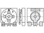
STEVAL-MKI205V1
STMicroelectronics
Position Sensor Development Tools LPS33W adapter board for a standard DIL24 sock
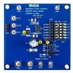
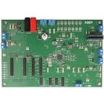
EV6545-V-00A
Monolithic Power Systems (MPS)
Power Management IC Development Tools 45V, 2.5A, Simple Three-Phase Power Stage Evaluation Board
| Distributor | SKU | Stock | MOQ | 1 | 10 | 50 | 100 | 1,000 | 10,000 |
|---|---|---|---|---|---|---|---|---|---|
| DigiKey | 1589-EV6545-V-00A-ND | 9 | 1 | $62.46 | $62.46 | $62.46 | $62.46 | $62.46 | $62.46 |
| AVNET Express | EV6545-V-00A | 0 | 1 | $68.64 | $61.68 | $60.00 | $60.00 | $60.00 | $60.00 |
| element14 APAC | EV6545-V-00A | 1 | 1 | * $63.27 | * $63.27 | * $63.27 | * $63.27 | * $63.27 | * $63.27 |
| Farnell | EV6545-V-00A | 1 | 1 | * $53.65 | * $53.65 | * $53.65 | * $53.65 | * $53.65 | * $53.65 |
| Mouser Electronics | 946-EV6545-V-00A | 10 | 1 | $62.40 | $62.40 | $62.40 | $62.40 | $62.40 | $62.40 |
| Newark | EV6545-V-00A | 1 | 1 | $71.39 | $71.39 | $71.39 | $71.39 | $71.39 | $71.39 |