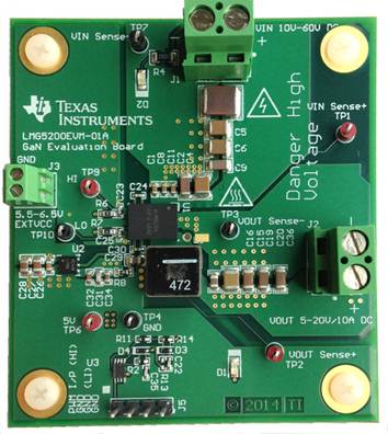
LMG5200 GaN Power Stage Evaluation Module
Texas Instruments
LMG5200 GaN Power Stage Evaluation Module
| Distributor | SKU | Stock | MOQ | 1 | 10 | 50 | 100 | 1,000 | 10,000 |
|---|---|---|---|---|---|---|---|---|---|
| AVNET Asia Pacific | LMG5200EVM-01A | 0 | 1 | $0.00 | $0.00 | $0.00 | $0.00 | $0.00 | $0.00 |
| AVNET Europe | LMG5200EVM-01A | 0 | 1 | * $0.00 | * $0.00 | * $0.00 | * $0.00 | * $0.00 | * $0.00 |
| AVNET Express | LMG5200EVM-01A | 0 | 1 | $0.00 | $0.00 | $0.00 | $0.00 | $0.00 | $0.00 |
| Mouser Electronics | N/A | 0 | |||||||
| Texas Instruments | LMG5200EVM-01A | 2 | $199.00 |
| Distributor | SKU | Stock | MOQ | 1 | 10 | 50 | 100 | 1,000 | 10,000 |
|---|---|---|---|---|---|---|---|---|---|
| DigiKey | TPS2023EVM-290-ND | 0 | $0.00 | $0.00 | $0.00 | $0.00 | $0.00 | $0.00 | |
| AVNET Express | TPS2023EVM-290 | 0 | 1 | $0.00 | $0.00 | $0.00 | $0.00 | $0.00 | $0.00 |
| element14 APAC | TPS2023EVM-290 | 0 | 1 | * $62.30 | * $62.30 | * $62.30 | * $62.30 | * $62.30 | * $62.30 |
| Farnell | TPS2023EVM-290 | 0 | 1 | * $56.09 | * $56.09 | * $56.09 | * $56.09 | * $56.09 | * $56.09 |
| Mouser Electronics | 595-TPS2023EVM-290 | 0 | 1 | ||||||
| Texas Instruments | TPS2023EVM-290 | 9 | $49.00 |
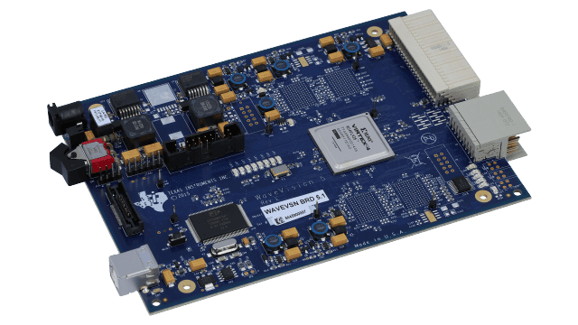
WaveVision 5 Data Capture Board Version 5.1
Texas Instruments
WaveVision 5 Data Capture Board Version 5.1
| Distributor | SKU | Stock | MOQ | 1 | 10 | 50 | 100 | 1,000 | 10,000 |
|---|---|---|---|---|---|---|---|---|---|
| DigiKey | 296-46024-ND | 3 | 1 | $1,498.80 | $1,498.80 | $1,498.80 | $1,498.80 | $1,498.80 | $1,498.80 |
| Mouser Electronics | N/A | 0 |
| Distributor | SKU | Stock | MOQ | 1 | 10 | 50 | 100 | 1,000 | 10,000 |
|---|---|---|---|---|---|---|---|---|---|
| DigiKey | 296-31226-ND | 0 | 1 | $61.25 | $61.25 | $61.25 | $61.25 | $61.25 | $61.25 |
| Arrow North American Components | TPS61150AEVM-150 | 0 | 1 | $56.54 | $58.64 | $58.64 | $57.69 | $0.00 | $0.00 |
| AVNET Europe | TPS61150AEVM-150 | 0 | 1 | * $0.00 | * $0.00 | * $0.00 | * $0.00 | * $0.00 | * $0.00 |
| AVNET Express | TPS61150AEVM-150 | 0 | 1 | $59.78 | $59.78 | $59.78 | $59.78 | $59.78 | $59.78 |
| Mouser Electronics | 595-TPS61150AEVM-150 | 0 | 1 | ||||||
| Texas Instruments | TPS61150AEVM-150 | 2 | 1 | $49.00 | $49.00 | $49.00 | $49.00 | $49.00 | $49.00 |
| Verical Marketplace | TPS61150AEVM-150 | 15 | 1 | $54.58 | $0.00 | $0.00 | $0.00 | $0.00 | $0.00 |
| Distributor | SKU | Stock | MOQ | 1 | 10 | 50 | 100 | 1,000 | 10,000 |
|---|---|---|---|---|---|---|---|---|---|
| Mouser Electronics | N/A | 0 |
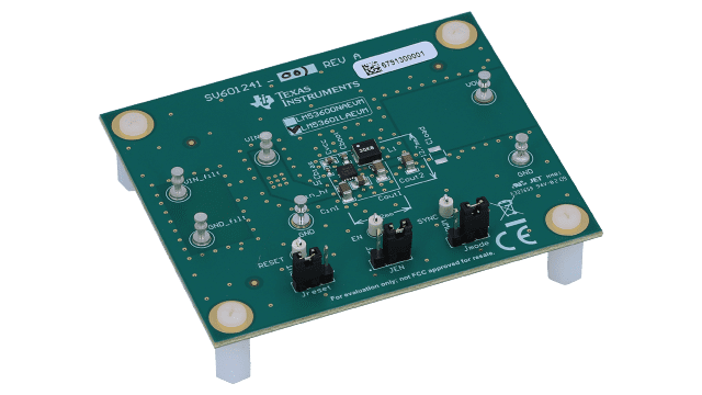
LM53601-Q1 5V Output; 1000mA Buck Regulator Evaluation Module With Spread Spectrum
Texas Instruments
LM53601-Q1 5V Output; 1000mA Buck Regulator Evaluation Module With Spread Spectrum
| Distributor | SKU | Stock | MOQ | 1 | 10 | 50 | 100 | 1,000 | 10,000 |
|---|---|---|---|---|---|---|---|---|---|
| DigiKey | 296-46733-ND | 1 | 1 | $58.80 | $58.80 | $58.80 | $58.80 | $58.80 | $58.80 |
| AVNET Express | LM53601LAEVM | 0 | 1 | $86.12 | $78.89 | $68.60 | $65.17 | $65.17 | $65.17 |
| Mouser Electronics | 595-LM53601LAEVM | 2 | 1 | $65.17 | $65.16 | $65.16 | $65.16 | $65.16 | $65.16 |
| Texas Instruments | LM53601LAEVM | 15 | 1 | $49.00 | $49.00 | $49.00 | $49.00 | $49.00 | $49.00 |
| Verical Marketplace | LM53601LAEVM | 13 | 1 | $62.27 | $56.61 | $55.18 | $55.18 | $55.18 | $55.18 |

| Distributor | SKU | Stock | MOQ | 1 | 10 | 50 | 100 | 1,000 | 10,000 |
|---|---|---|---|---|---|---|---|---|---|
| DigiKey | 296-19911-ND | 0 | 1 | $53.43 | $53.43 | $53.43 | $53.43 | $53.43 | $53.43 |
| Mouser Electronics | 595-ADS7816EVM | 0 | 1 | ||||||
| Texas Instruments | ADS7816EVM | 18 | $49.00 | ||||||
| Win Source | ADS7816EVM | 1 | 21 |
8-Bit, 1MSPS SAR ADC Performance Demonstration Kit
Texas Instruments
8-Bit, 1MSPS SAR ADC Performance Demonstration Kit
| Distributor | SKU | Stock | MOQ | 1 | 10 | 50 | 100 | 1,000 | 10,000 |
|---|---|---|---|---|---|---|---|---|---|
| DigiKey | 296-39575-ND | 1 | 1 | $210.14 | $210.14 | $210.14 | $210.14 | $210.14 | $210.14 |
| Arrow North American Components | ADS7040EVM-PDK | 0 | 1 | $0.00 | $227.39 | $227.39 | $203.66 | $203.66 | $202.72 |
| AVNET Express | ADS7040EVM-PDK | 0 | 1 | $0.00 | $0.00 | $0.00 | $0.00 | $0.00 | $0.00 |
| element14 APAC | ADS7040EVM-PDK | 0 | 1 | * $244.10 | * $244.10 | * $244.10 | * $244.10 | * $244.10 | * $244.10 |
| Farnell | ADS7040EVM-PDK | 1 | 1 | * $215.78 | * $215.78 | * $215.78 | * $215.78 | * $215.78 | * $215.78 |
| Mouser Electronics | 595-ADS7040EVM-PDK | 1 | 1 | $232.92 | $232.92 | $232.92 | $232.92 | $232.92 | $232.92 |
| Texas Instruments | ADS7040EVM-PDK | 23 | 1 | $199.00 | $199.00 | $199.00 | $199.00 | $199.00 | $199.00 |
| Verical Marketplace | ADS7040EVM-PDK | 12 | 1 | $253.32 | $253.32 | $253.32 | $253.32 | $253.32 | $253.32 |
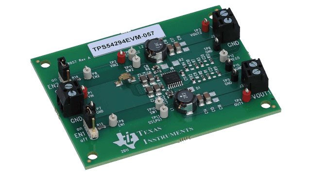
Evaluation Module for TPS54294 Synchronous Step-Down Converter
Texas Instruments
Evaluation Module for TPS54294 Synchronous Step-Down Converter
| Distributor | SKU | Stock | MOQ | 1 | 10 | 50 | 100 | 1,000 | 10,000 |
|---|---|---|---|---|---|---|---|---|---|
| DigiKey | 296-31188-ND | 1 | 1 | $61.25 | $61.25 | $61.25 | $61.25 | $61.25 | $61.25 |
| Arrow North American Components | TPS54294EVM-057 | 0 | 1 | $67.98 | $67.30 | $65.96 | $65.30 | $63.37 | $62.73 |
| AVNET Express | TPS54294EVM-057 | 0 | 1 | $59.78 | $59.78 | $59.78 | $59.78 | $59.78 | $59.78 |
| element14 APAC | TPS54294EVM-057 | 0 | 1 | * $60.96 | * $60.96 | * $60.96 | * $60.96 | * $60.96 | * $60.96 |
| Farnell | TPS54294EVM-057 | 2 | 1 | * $58.07 | * $58.07 | * $58.07 | * $58.07 | * $58.07 | * $58.07 |
| Mouser Electronics | 595-TPS54294EVM-057 | 0 | 1 | $63.71 | $63.71 | $63.71 | $63.71 | $63.71 | $63.71 |
| Newark | TPS54294EVM-057 | 0 | 1 | $50.73 | $50.73 | $50.73 | $50.73 | $50.73 | $50.73 |
| Texas Instruments | TPS54294EVM-057 | 31 | 1 | $49.00 | $49.00 | $49.00 | $49.00 | $49.00 | $49.00 |
| Verical Marketplace | TPS54294EVM-057 | 43 | 1 | $54.58 | $54.58 | $54.58 | $54.58 | $54.58 | $54.58 |
| Distributor | SKU | Stock | MOQ | 1 | 10 | 50 | 100 | 1,000 | 10,000 |
|---|---|---|---|---|---|---|---|---|---|
| DigiKey | 296-38887-ND | 3 | 1 | $311.25 | $311.25 | $311.25 | $311.25 | $311.25 | $311.25 |
| Arrow North American Components | BQ76930EVM | 0 | 1 | $345.47 | $342.01 | $335.21 | $331.85 | $322.00 | $318.78 |
| AVNET Europe | BQ76930EVM | 0 | 1 | * $310.21 | * $306.23 | * $298.61 | * $294.97 | * $294.97 | * $294.97 |
| AVNET Express | BQ76930EVM | 0 | 1 | $303.78 | $303.78 | $303.78 | $303.78 | $303.78 | $303.78 |
| element14 APAC | BQ76930EVM | 6 | 1 | * $356.18 | * $356.18 | * $356.18 | * $356.18 | * $356.18 | * $356.18 |
| Farnell | BQ76930EVM | 6 | 1 | * $298.04 | * $298.04 | * $298.04 | * $298.04 | * $298.04 | * $298.04 |
| Mouser Electronics | 595-BQ76930EVM | 8 | 1 | $323.73 | $323.73 | $323.73 | $323.73 | $323.73 | $323.73 |
| Newark | BQ76930EVM | 6 | 1 | $314.07 | $306.71 | $306.71 | $306.71 | $306.71 | $306.71 |
| Texas Instruments | BQ76930EVM | 29 | 1 | $249.00 | $249.00 | $249.00 | $249.00 | $249.00 | $249.00 |
| Verical Marketplace | BQ76930EVM | 1 | 1 | $292.56 | $312.93 | $312.93 | $312.93 | $312.93 | $312.93 |