



ADV3228-EVALZ
Analog Devices Inc.
The ADV3228/ADV3229 are high speed 8 ? 8 analog crosspoint switch matrices. They offer a ?3 dB large signal bandwidth of 750 MHz (ADV3228) and a slew rate of 2500 V/?s.The ADV3228/ADV3229 include eight independent output buffers that can be placed into a high impedance state for paralleling crosspoint outputs to prevent off channels from loading the output bus. The ADV3228 has a gain of +1, the ADV3229 has a gain of +2, and they both operate on voltage supplies of ?5 V. Channel switching is performed via a serial digital control that can accommodate daisy chaining of several devices or via a parallel control to allow updating of an individual output without reprogramming the entire array.The ADV3228/ADV3229 are available in the 72-lead LFCSP package over the extended industrial temperature range of ?40?C to +85?C.Applications Routing of high speed signals including: ? ? ? Video (NTSC, PAL, S, SECAM, YUV, RGB) ? ? ? Compressed video (MPEG, wavelet) ? ? ? 3-level digital video (HDB3) Data communications Telecommunications
| Distributor | SKU | Stock | MOQ | 1 | 10 | 50 | 100 | 1,000 | 10,000 |
|---|---|---|---|---|---|---|---|---|---|
| Mouser Electronics | N/A | 0 |
 Manufacturer Page
DC082B
Analog Devices Inc.
The LT1182/LT1183 are dual current mode switching regulators that provide the control function for Cold Cathode Fluorescent Lighting (CCFL) and Liquid Crystal Display (LCD) Contrast. The LT1184/LT1184F provide only the CCFL function. The ICs include high current, high efficiency switches, an oscillator, a reference, output drive logic, control blocks and protection circuitry. The LT1182 permits positive or negative voltage LCD contrast operation. The LT1183 permits unipolar contrast operation and pins out an internal reference. The LT1182/LT1183 support grounded and floating lamp configurations. The LT1184F supports grounded and floating lamp configurations. The LT1184 supports only grounded lamp configurations.Applications Notebook and Palmtop Computers Portable Instruments Automotive Displays Retail Terminals
| Distributor | SKU | Stock | MOQ | 1 | 10 | 50 | 100 | 1,000 | 10,000 |
|---|---|---|---|---|---|---|---|---|---|
| Mouser Electronics | N/A | 0 |

AD9231-20EBZ
Analog Devices Inc.
The AD9231 is a monolithic, dual-channel, 1.8 V supply, 12-bit, 20 MSPS / 40?MSPS / 65 MSPS/80 MSPS analog-to-digital converter (ADC). It features a high performance sample-and-hold circuit and on-chip voltage reference.The product uses multistage differential pipeline architecture with output error correction logic to provide 12-bit accuracy at 80 MSPS data rates and to guarantee no missing codes over the full operating temperature range.The ADC contains several features designed to maximize flexibility and minimize system cost, such as programmable clock and data alignment and programmable digital test pattern generation. The available digital test patterns include built-in deterministic and pseudorandom patterns, along with custom user-defined test patterns entered via the serial port interface (SPI).A differential clock input controls all internal conversion cycles. An optional duty cycle stabilizer (DCS) compensates for wide variations in the clock duty cycle while maintaining excellent overall ADC performance.The digital output data is presented in offset binary, gray code, or twos complement format. A data output clock (DCO) is provided for each ADC channel to ensure proper latch timing with receiving logic. Both 1.8 V and 3.3 V CMOS levels are supported, and output data can be multiplexed onto a single output bus.The AD9231 is available in a 64-lead RoHS compliant LFCSP and is specified over the industrial temperature range (?40?C to +85?C).PRODUCT HIGHLIGHTS The AD9231 operates from a single 1.8 V analog power supply and features a separate digital output driver supply to accommodate 1.8 V to 3.3 V logic families. The patented sample-and-hold circuit maintains excellent performance for input frequencies up to 200 MHz and is designed for low cost, low power, and ease of use. A standard serial port interface supports various product features and functions, such as data output formatting, internal clock divider, power-down, DCO/DATA timing and offset adjustments, and voltage reference modes. The AD9231 is packaged in a 64-lead RoHS compliant LFCSP that is pin compatible with the AD9268 16-bit ADC, the AD9258 14-bit ADC, the AD9251 14-bit ADC, and the AD9204 10-bit ADC, enabling a simple migration path between 10-bit and 16-bit converters sampling from 20 MSPS to 125 MSPS.?APPLICATIONS Communications Diversity radio systems Multimode digital receivers GSM, EDGE, W-CDMA, LTE, CDMA2000, WiMAX, TD-SCDMA I/Q demodulation systems Smart antenna systems Battery-powered instruments Hand held scope meters Portable medical imaging Ultrasound Radar/LIDAR
| Distributor | SKU | Stock | MOQ | 1 | 10 | 50 | 100 | 1,000 | 10,000 |
|---|---|---|---|---|---|---|---|---|---|
| Mouser Electronics | N/A | 0 |
AD9231-40EBZ
Analog Devices Inc.
The AD9231 is a monolithic, dual-channel, 1.8 V supply, 12-bit, 20 MSPS / 40?MSPS / 65 MSPS/80 MSPS analog-to-digital converter (ADC). It features a high performance sample-and-hold circuit and on-chip voltage reference.The product uses multistage differential pipeline architecture with output error correction logic to provide 12-bit accuracy at 80 MSPS data rates and to guarantee no missing codes over the full operating temperature range.The ADC contains several features designed to maximize flexibility and minimize system cost, such as programmable clock and data alignment and programmable digital test pattern generation. The available digital test patterns include built-in deterministic and pseudorandom patterns, along with custom user-defined test patterns entered via the serial port interface (SPI).A differential clock input controls all internal conversion cycles. An optional duty cycle stabilizer (DCS) compensates for wide variations in the clock duty cycle while maintaining excellent overall ADC performance.The digital output data is presented in offset binary, gray code, or twos complement format. A data output clock (DCO) is provided for each ADC channel to ensure proper latch timing with receiving logic. Both 1.8 V and 3.3 V CMOS levels are supported, and output data can be multiplexed onto a single output bus.The AD9231 is available in a 64-lead RoHS compliant LFCSP and is specified over the industrial temperature range (?40?C to +85?C).PRODUCT HIGHLIGHTS The AD9231 operates from a single 1.8 V analog power supply and features a separate digital output driver supply to accommodate 1.8 V to 3.3 V logic families. The patented sample-and-hold circuit maintains excellent performance for input frequencies up to 200 MHz and is designed for low cost, low power, and ease of use. A standard serial port interface supports various product features and functions, such as data output formatting, internal clock divider, power-down, DCO/DATA timing and offset adjustments, and voltage reference modes. The AD9231 is packaged in a 64-lead RoHS compliant LFCSP that is pin compatible with the AD9268 16-bit ADC, the AD9258 14-bit ADC, the AD9251 14-bit ADC, and the AD9204 10-bit ADC, enabling a simple migration path between 10-bit and 16-bit converters sampling from 20 MSPS to 125 MSPS.?APPLICATIONS Communications Diversity radio systems Multimode digital receivers GSM, EDGE, W-CDMA, LTE, CDMA2000, WiMAX, TD-SCDMA I/Q demodulation systems Smart antenna systems Battery-powered instruments Hand held scope meters Portable medical imaging Ultrasound Radar/LIDAR
| Distributor | SKU | Stock | MOQ | 1 | 10 | 50 | 100 | 1,000 | 10,000 |
|---|---|---|---|---|---|---|---|---|---|
| Mouser Electronics | N/A | 0 |

AD9258-80EBZ
Analog Devices Inc.
The AD9258 is a dual, 14-bit, 80 MSPS/105 MSPS/125 MSPS analog-to-digital converter (ADC). The AD9258 is designed to support communications applications where high performance, combined with low cost, small size, and versatility, is desired.The dual ADC core features a multistage, differential pipelined architecture with integrated output error correction logic. Each ADC features wide bandwidth differential sample-and-hold analog input amplifiers that support a variety of user-selectable input ranges. An integrated voltage reference eases design considerations. A duty cycle stabilizer is provided to compensate for variations in the ADC clock duty cycle, allowing the converters to maintain excellent performance.The ADC output data can be routed directly to the two external 14-bit output ports. These outputs can be set to either 1.8 V CMOS or LVDS.Flexible power-down options allow significant power savings, when desired.Programming for setup and control is accomplished using a 3-wire SPI-compatible serial interface.The AD9258 is available in a 64-lead LFCSP and is specified over the industrial temperature range of ?40?C to +85?C.PRODUCT HIGHLIGHTS On-chip dither option for improved SFDR performance with low power analog input. Proprietary differential input that maintains excellent SNR performance for input frequencies up to 300 MHz. Operation from a single 1.8 V supply and a separate digital output driver supply accommodating 1.8 V CMOS or LVDS outputs. Standard serial port interface (SPI) that supports various product features and functions, such as data formatting (offset binary, twos complement, or gray coding), enabling the clock DCS, power-down, test modes, and voltage reference mode. Pin compatibility with the AD9268, allowing a simple migration from 14 bits to 16 bits. The AD9258 is also pin compatible with the AD9251, AD9231, and AD9204 family of products for lower sample rate, low power applications.APPLICATIONS Communications Diversity radio systems Multimode digital receivers (3G) GSM, EDGE, W-CDMA, LTE, CDMA2000, WiMAX, TD-SCDMA I/Q demodulation systems Smart antenna systems General-purpose software radios Broadband data applications Ultrasound Equipment
| Distributor | SKU | Stock | MOQ | 1 | 10 | 50 | 100 | 1,000 | 10,000 |
|---|---|---|---|---|---|---|---|---|---|
| Mouser Electronics | N/A | 0 |

AD9287-100KITZ
Analog Devices Inc.
The AD9287 is a quad, 8-bit, 100 MSPS analog-to-digital con-verter (ADC) with an on-chip sample-and-hold circuit designedfor low cost, low power, small size, and ease of use. The productoperates at a conversion rate of up to 100 MSPS and is optimized for outstanding dynamic performance and low power in applications where a small package size is critical.The ADC requires a single 1.8 V power supply and LVPECL-/ CMOS-/LVDS-compatible sample rate clock for full performanceoperation. No external reference or driver components arerequired for many applications.The ADC automatically multiplies the sample rate clock for theappropriate LVDS serial data rate. A data clock output (DCO) for capturing data on the output and a frame clock output (FCO) for signaling a new output byte are provided. Individual-channel power-down is supported and typically consumes less than 2 mW when all channels are disabled.The ADC contains several features designed to maximizeflexibility and minimize system cost, such as programmableclock and data alignment and programmable digital test patterngeneration. The available digital test patterns include built-in deterministic and pseudorandom patterns, along with custom user-defined test patterns entered via the serial port interface (SPI).The AD9287 is available in an RoHS compliant, 48-lead LFCSP. It isspecified over the industrial temperature range of ?40?C to +85?C.Product Highlights Small Footprint. Four ADCs are contained in a small, space-saving package. Low power of 133 mW/channel at 100 MSPS. Ease of Use. A data clock output (DCO) is provided that operates at frequencies of up to 400 MHz and supports double data rate (DDR) operation. User Flexibility. The SPI control offers a wide range of flexible features to meet specific system requirements. Pin-Compatible Family. This includes the AD9219 (10-bit), AD9228 (12-bit), and AD9259 (14-bit).ApplicationsMedical imaging and nondestructive ultrasoundPortable ultrasound and digital beam-forming systemsQuadrature radio receiversDiversity radio receiversTape drivesOptical networkingTest equipment
| Distributor | SKU | Stock | MOQ | 1 | 10 | 50 | 100 | 1,000 | 10,000 |
|---|---|---|---|---|---|---|---|---|---|
| Mouser Electronics | N/A | 0 |

AD9572-EVALZ-PEC
Analog Devices Inc.
The AD9572 provides a multioutput clock generator function along with two on-chip PLL cores, optimized for fiber channel line card applications that include an Ethernet interface. The integer-N PLL design is based on the Analog Devices, Inc., proven portfolio of high performance, low jitter frequencysynthesizers to maximize network performance. Other applications with demanding phase noise and jitter requirements also benefit from this part. The PLL section consists of a low noise phase frequency detector (PFD), a precision charge pump (CP), a low phase noise voltage controlled oscillator (VCO), and a preprogrammed feedback divider and output divider. By connecting an external crystal or reference clock to the REFCLK pin, frequencies up to 156.25 MHz can be locked to the input reference. Each output divider and feedback divider ratio is preprogrammed for therequired output rates. A second PLL also operates as an integer-N synthesizer anddrives two LVPECL or LVDS output buffers for 106.25 MHzoperation. No external loop filter components are required, thusconserving valuable design time and board space. The AD9572 is available in a 40-lead, 6 mm ? 6 mm lead framechip scale package (LFCSP) and can be operated from a single3.3 V supply. The temperature range is ?40?C to +85?C.APPLICATIONSFiber channel line cards, switches, and routersGigabit Ethernet/PCIe support included Low jitter, low phase noise clock generation
| Distributor | SKU | Stock | MOQ | 1 | 10 | 50 | 100 | 1,000 | 10,000 |
|---|---|---|---|---|---|---|---|---|---|
| Mouser Electronics | N/A | 0 |

| Distributor | SKU | Stock | MOQ | 1 | 10 | 50 | 100 | 1,000 | 10,000 |
|---|---|---|---|---|---|---|---|---|---|
| Mouser Electronics | N/A | 0 |

ADMV4821-EVALZ
Analog Devices Inc.
The ADMV4821 is a silicon germanium (SiGe), 24 GHz millimeterwave (mmW) to 29.5 GHz mmW 5G beamformer. The RF IC is highly integrated and contains 16 independent channels with both transmit and receive functionality. The ADMV4821 supports eight horizontal and eight vertical polarized antennas via the independent RFV and RFH inputs/outputs common pins.In transmit mode, both the RFV and RFH input signals are split via two independent 1:8 power splitters and pass through the eight, independent, corresponding transmit channels. In this mode, each channel includes a vector modulator (VM) to control the phase and two digital variable gain amplifiers (DVGAs) to control the amplitude.In receive mode, input signals pass through two sets of eight receive channels (either vertical or horizontal) and are combined via one independent 8:1 combiner connected to the RFV pin and one independent 8:1 combiner connected to the RFH pin. In this mode, each channel includes a VM to control the phase and a DVGA to control the amplitude.The VM provides a full 360? phase adjustment range in either transmit or receive mode. The VM provides six bits of resolution for 5.625? phase steps.In transmit mode, the total DVGA dynamic range adjustment range is 32.4 dB. The DVGAs provide five bits or six bits of resolution, resulting in 1.0 dB or 0.5 dB amplitude steps, respectively.In receive mode, the DVGA allows for 17.1 dB of dynamic range adjustment. The DVGA also provides six bits of resolution, resulting in 0.5 dB amplitude steps. The DVGAs provide a flat phase response across the full gain range.The transmitter channels contain individual power detectors to detect and calibrate the gain for each channel as well as the channel to channel gain mismatch. Directly connect the ADMV4821 RF ports to a patch antenna to create a dual polarization mmW 5G subarray.Users can program the ADMV4821 by using a 3-wire or 4-wire serial port interface (SPI). The integrated on-chip low dropout (LDO) regulator generates the 1.8 V supply for the SPI circuitry to reduce the number of supply domains required. There are various SPI modes to enable fast startup and control during normal operation.Users can either set the amplitude and phase for each channel individually or program multiple channels simultaneously by using the on-chip memory for beamforming. The on-chip memory can store up to 256 beam positions, which can be allocated for either transmitter or receiver mode in any combination. In addition, four address pins allow SPI control of up to 16 devices on the same serial lines. Dedicated horizontal and vertical polarization load pins also synchronize all devices in the same array. There is a horizontal and vertical polarization transmit and receive mode control pins (TRXV and TRXH) for fast switching between transmit and receive mode.The ADMV4821 comes in a compact, thermally enhanced 10 mm ? 10 mm, RoHs compliant land grid array (LGA) package. The ADMV4821 operates over the ?40?C to +95?C case temperature range. This LGA package allows users to heat-sink the ADMV4821 from the top side of the package for the most efficient thermal heatsinking and to allow flexible antenna placement on the opposite side of the printed circuit board (PCB).Throughout the figures in the data sheet, Tx means transmit (or transmitter) and Rx means receive (or receiver).APPLICATIONS5G applicationsBroadband communicationTest and measurementAerospace and defense
| Distributor | SKU | Stock | MOQ | 1 | 10 | 50 | 100 | 1,000 | 10,000 |
|---|---|---|---|---|---|---|---|---|---|
| Mouser Electronics | N/A | 0 |
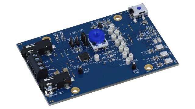
| Distributor | SKU | Stock | MOQ | 1 | 10 | 50 | 100 | 1,000 | 10,000 |
|---|---|---|---|---|---|---|---|---|---|
| DigiKey | 296-31037-ND | 9 | 1 | $123.75 | $123.75 | $123.75 | $123.75 | $123.75 | $123.75 |
| Arrow North American Components | TLV320AIC3120EVM-U | 0 | 1 | $134.49 | $133.14 | $130.49 | $129.19 | $125.35 | $124.10 |
| AVNET Express | TLV320AIC3120EVM-U | 0 | 1 | $91.50 | $91.50 | $91.50 | $91.50 | $91.50 | $91.50 |
| element14 APAC | TLV320AIC3120EVM-U | 0 | 1 | * $95.06 | * $95.06 | * $95.06 | * $95.06 | * $95.06 | * $95.06 |
| Farnell | TLV320AIC3120EVM-U | 0 | 1 | * $99.32 | * $99.32 | * $99.32 | * $99.32 | * $99.32 | * $99.32 |
| Mouser Electronics | 595-LV320AIC3120EVMU | 8 | 1 | $128.71 | $128.71 | $128.71 | $128.71 | $128.71 | $128.71 |
| Newark | TLV320AIC3120EVM-U | 0 | 1 | $77.65 | $77.65 | $77.65 | $77.65 | $77.65 | $77.65 |
| Texas Instruments | TLV320AIC3120EVM-U | 52 | 1 | $99.00 | $99.00 | $99.00 | $99.00 | $99.00 | $99.00 |
| Verical Marketplace | TLV320AIC3120EVM-U | 1 | 1 | $86.16 | $86.16 | $86.16 | $86.16 | $86.16 | $86.16 |