Evaluation Module for TPS65258, Three DC-DC converters with Integrated FET and 2 USB Switches
Texas Instruments
Evaluation Module for TPS65258, Three DC-DC converters with Integrated FET and 2 USB Switches
| Distributor | SKU | Stock | MOQ | 1 | 10 | 50 | 100 | 1,000 | 10,000 |
|---|---|---|---|---|---|---|---|---|---|
| DigiKey | 296-31279-ND | 0 | |||||||
| Arrow North American Components | TPS65258EVM | 0 | 1 | $0.00 | $50.67 | $50.67 | $50.30 | $47.66 | $47.66 |
| AVNET Express | TPS65258EVM | 0 | 1 | $0.00 | $0.00 | $0.00 | $0.00 | $0.00 | $0.00 |
| Farnell | TPS65258EVM | 2 | $1.00 | ||||||
| Mouser Electronics | 595-TPS65258EVM | 1 | 1 | $57.07 | $57.06 | $57.06 | $57.06 | $57.06 | $57.06 |
| Newark | TPS65258EVM | 2 | 1 | $50.73 | $50.73 | $50.73 | $50.73 | $50.73 | $50.73 |
| Texas Instruments | TPS65258EVM | 29 | 1 | $49.00 | $49.00 | $49.00 | $49.00 | $49.00 | $49.00 |
| Verical Marketplace | TPS65258EVM | 1 | 1 | $62.38 | $62.38 | $62.38 | $62.38 | $62.38 | $62.38 |
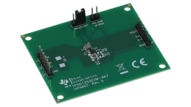
Evaluation Module Board for TPS61252 3.5MHz; 1.5A; 92% Efficient Step-up (Boost) Converter
Texas Instruments
Evaluation Module Board for TPS61252 3.5MHz; 1.5A; 92% Efficient Step-up (Boost) Converter
| Distributor | SKU | Stock | MOQ | 1 | 10 | 50 | 100 | 1,000 | 10,000 |
|---|---|---|---|---|---|---|---|---|---|
| DigiKey | 296-31242-ND | 2 | 1 | $61.25 | $61.25 | $61.25 | $61.25 | $61.25 | $61.25 |
| Arrow North American Components | TPS61252EVM-667 | 0 | 1 | $66.72 | $66.05 | $64.74 | $64.09 | $62.19 | $61.56 |
| AVNET Express | TPS61252EVM-667 | 0 | 1 | $59.78 | $59.78 | $59.78 | $59.78 | $59.78 | $59.78 |
| element14 APAC | TPS61252EVM-667 | 0 | 1 | * $61.35 | * $61.35 | * $61.35 | * $61.35 | * $61.35 | * $61.35 |
| Farnell | TPS61252EVM-667 | 0 | 1 | * $66.11 | * $66.11 | * $66.11 | * $66.11 | * $66.11 | * $66.11 |
| Mouser Electronics | 595-TPS61252EVM-667 | 1 | 1 | $63.71 | $63.71 | $63.71 | $63.71 | $63.71 | $63.71 |
| Newark | TPS61252EVM-667 | 0 | 1 | $50.73 | $50.73 | $50.73 | $50.73 | $50.73 | $50.73 |
| Texas Instruments | TPS61252EVM-667 | 25 | 1 | $49.00 | $49.00 | $49.00 | $49.00 | $49.00 | $49.00 |
| Verical Marketplace | TPS61252EVM-667 | 1 | 1 | $56.29 | $0.00 | $0.00 | $0.00 | $0.00 | $0.00 |
| Win Source | TPS61252EVM-667 | 550 | 1 |
| Distributor | SKU | Stock | MOQ | 1 | 10 | 50 | 100 | 1,000 | 10,000 |
|---|---|---|---|---|---|---|---|---|---|
| DigiKey | 296-19719-ND | 5 | 1 | $58.80 | $58.80 | $58.80 | $58.80 | $58.80 | $58.80 |
| Arrow North American Components | BQ24120EVM-001 | 0 | 1 | $66.57 | $65.90 | $64.59 | $63.94 | $62.04 | $61.42 |
| element14 APAC | BQ24120EVM-001 | 2 | 1 | * $83.27 | * $83.27 | * $83.27 | * $83.27 | * $83.27 | * $83.27 |
| Farnell | BQ24120EVM-001 | 2 | 1 | * $66.11 | * $66.11 | * $66.11 | * $66.11 | * $66.11 | * $66.11 |
| Mouser Electronics | 595-BQ24120EVM-001 | 2 | 1 | $65.17 | $65.16 | $65.16 | $65.16 | $65.16 | $65.16 |
| Newark | BQ24120EVM-001 | 2 | 6 | $20.93 | $20.93 | $20.93 | $20.93 | $20.93 | $20.93 |
| Texas Instruments | BQ24120EVM-001 | 14 | 1 | $49.00 | $49.00 | $49.00 | $49.00 | $49.00 | $49.00 |
| Verical Marketplace | BQ24120EVM-001 | 27 | 1 | $54.59 | $54.59 | $54.59 | $54.59 | $54.59 | $54.59 |
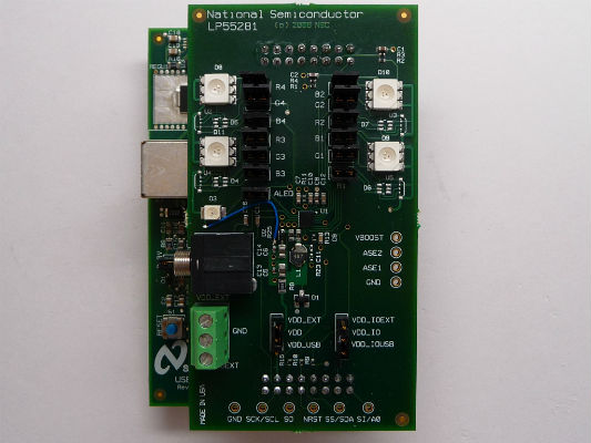
Quad RGB Driver from the PowerWise® Family
Texas Instruments
Quad RGB Driver from the PowerWise® Family
| Distributor | SKU | Stock | MOQ | 1 | 10 | 50 | 100 | 1,000 | 10,000 |
|---|---|---|---|---|---|---|---|---|---|
| DigiKey | LP55281RLEV-ND | 0 | 1 | $106.98 | $106.98 | $106.98 | $106.98 | $106.98 | $106.98 |
| Mouser Electronics | 926-LP55281RLEV | 0 | 1 |
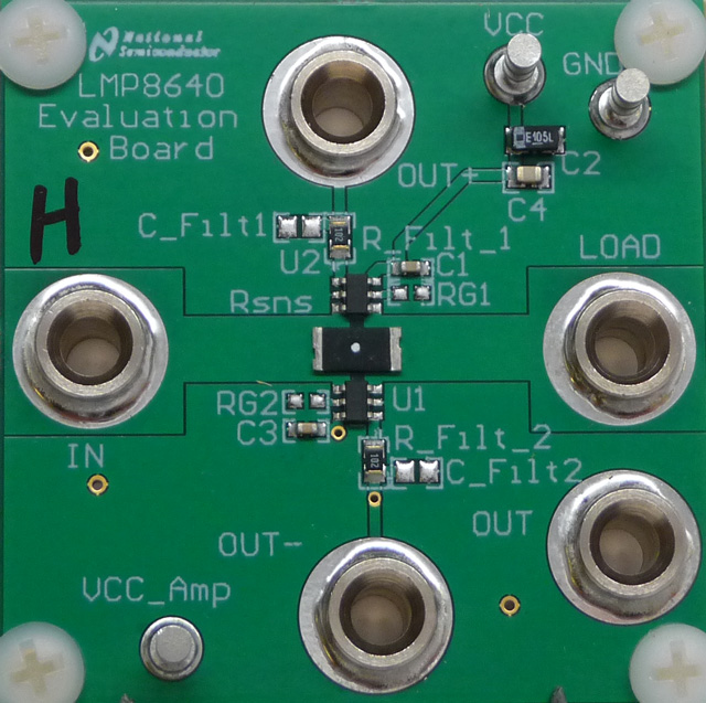
Evaluation board for LMP8640HV-H – 100V/V
Texas Instruments
Evaluation board for LMP8640HV-H – 100V/V
| Distributor | SKU | Stock | MOQ | 1 | 10 | 50 | 100 | 1,000 | 10,000 |
|---|---|---|---|---|---|---|---|---|---|
| DigiKey | 296-49757-ND | 2 | 1 | $94.43 | $79.76 | $72.27 | $69.59 | $69.59 | $69.59 |
| Mouser Electronics | N/A | 0 |
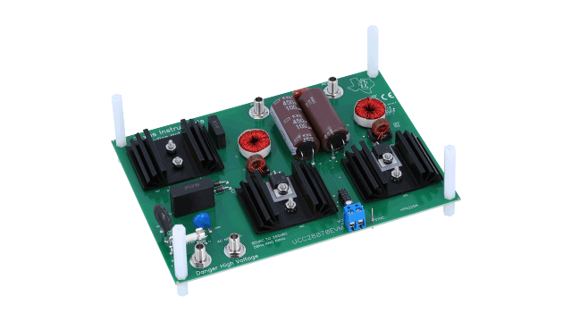
| Distributor | SKU | Stock | MOQ | 1 | 10 | 50 | 100 | 1,000 | 10,000 |
|---|---|---|---|---|---|---|---|---|---|
| DigiKey | 296-31338-ND | 6 | 1 | $118.80 | $118.80 | $118.80 | $118.80 | $118.80 | $118.80 |
| Arrow Asia | UCC28070EVM | 1 | 1 | $118.02 | $0.00 | $0.00 | $0.00 | $0.00 | $0.00 |
| Arrow North American Components | UCC28070EVM | 0 | 1 | $134.67 | $133.32 | $130.67 | $129.36 | $125.52 | $124.27 |
| AVNET Europe | UCC28070EVM | 0 | 1 | * $169.01 | * $163.92 | * $151.70 | * $144.57 | * $144.57 | * $144.57 |
| AVNET Express | UCC28070EVM | 0 | 1 | $120.78 | $120.78 | $120.78 | $120.78 | $120.78 | $120.78 |
| element14 APAC | UCC28070EVM | 1 | 1 | * $147.63 | * $147.63 | * $147.63 | * $147.63 | * $147.63 | * $147.63 |
| Farnell | UCC28070EVM | 1 | 1 | * $151.49 | * $151.49 | * $151.49 | * $151.49 | * $151.49 | * $151.49 |
| Mouser Electronics | 595-UCC28070EVM | 7 | 1 | $128.71 | $128.71 | $128.71 | $128.71 | $128.71 | $128.71 |
| Newark | UCC28070EVM | 1 | 1 | $132.19 | $129.09 | $129.09 | $129.09 | $129.09 | $129.09 |
| Texas Instruments | UCC28070EVM | 40 | 1 | $99.00 | $99.00 | $99.00 | $99.00 | $99.00 | $99.00 |
| Verical Marketplace | UCC28070EVM | 1 | 1 | $113.74 | $0.00 | $0.00 | $0.00 | $0.00 | $0.00 |
| Win Source | UCC28070EVM | 2 | 1 |
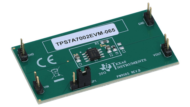
TPS7A7002 Low-Dropout (LDO) Linear Regulator Evaluation Module
Texas Instruments
TPS7A7002 Low-Dropout (LDO) Linear Regulator Evaluation Module
| Distributor | SKU | Stock | MOQ | 1 | 10 | 50 | 100 | 1,000 | 10,000 |
|---|---|---|---|---|---|---|---|---|---|
| DigiKey | 296-45970-ND | 2 | 1 | $24.00 | $24.00 | $24.00 | $24.00 | $24.00 | $24.00 |
| Arrow North American Components | TPS7A7002EVM-065 | 0 | 1 | $27.85 | $27.57 | $27.02 | $26.75 | $25.96 | $25.70 |
| AVNET Express | TPS7A7002EVM-065 | 0 | 1 | $24.40 | $24.40 | $24.40 | $24.40 | $24.40 | $24.40 |
| Mouser Electronics | 595-TPS7A7002EVM-065 | 5 | 1 | $26.00 | $26.00 | $26.00 | $26.00 | $26.00 | $26.00 |
| Newark | TPS7A7002EVM-065 | 0 | 1 | $20.71 | $20.71 | $20.71 | $20.71 | $20.71 | $20.71 |
| Texas Instruments | TPS7A7002EVM-065 | 36 | 1 | $20.00 | $20.00 | $20.00 | $20.00 | $20.00 | $20.00 |
| Verical Marketplace | TPS7A7002EVM-065 | 3 | 2 | $22.28 | $22.28 | $22.28 | $22.28 | $22.28 |
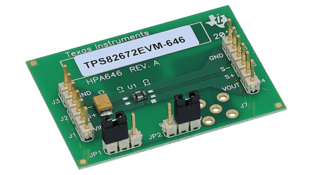
Evaluation Module for TPS82672 600-mA; High-Efficiency MicroSiP Step-Down Converter
Texas Instruments
Evaluation Module for TPS82672 600-mA; High-Efficiency MicroSiP Step-Down Converter
| Distributor | SKU | Stock | MOQ | 1 | 10 | 50 | 100 | 1,000 | 10,000 |
|---|---|---|---|---|---|---|---|---|---|
| DigiKey | 296-30303-ND | 0 | |||||||
| Arrow North American Components | TPS82672EVM-646 | 0 | 1 | $23.08 | $23.91 | $23.91 | $23.35 | $20.56 | $20.56 |
| AVNET Express | TPS82672EVM-646 | 0 | 1 | $24.40 | $24.40 | $24.40 | $24.40 | $24.40 | $24.40 |
| Mouser Electronics | 595-TPS82672EVM-646 | 0 | 1 | $26.00 | $26.00 | $26.00 | $26.00 | $26.00 | $26.00 |
| Newark | TPS82672EVM-646 | 0 | 1 | $20.71 | $20.71 | $20.71 | $20.71 | $20.71 | $20.71 |
| Texas Instruments | TPS82672EVM-646 | 22 | 1 | $20.00 | $20.00 | $20.00 | $20.00 | $20.00 | $20.00 |
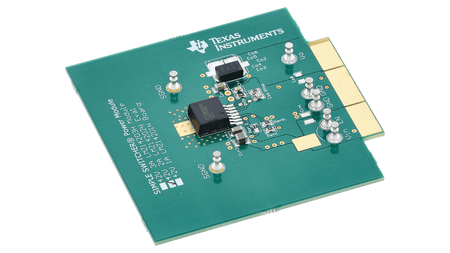
SIMPLE SWITCHER® Power Module 42Vin; High Output Voltage 2A Eval Board
Texas Instruments
SIMPLE SWITCHER® Power Module 42Vin; High Output Voltage 2A Eval Board
| Distributor | SKU | Stock | MOQ | 1 | 10 | 50 | 100 | 1,000 | 10,000 |
|---|---|---|---|---|---|---|---|---|---|
| DigiKey | LMZ14202HEVAL/NOPB-ND | 1 | 1 | $58.80 | $58.80 | $58.80 | $58.80 | $58.80 | $58.80 |
| Mouser Electronics | N/A | 0 |
150mA; 100V Wide Vin Step-Down Switching Regulator Evaluation Module
Texas Instruments
150mA; 100V Wide Vin Step-Down Switching Regulator Evaluation Module
| Distributor | SKU | Stock | MOQ | 1 | 10 | 50 | 100 | 1,000 | 10,000 |
|---|---|---|---|---|---|---|---|---|---|
| DigiKey | LM5009EVAL-ND | 0 | 1 | $44.15 | $44.15 | $44.15 | $44.15 | $44.15 | $44.15 |
| Mouser Electronics | N/A | 0 |