| Distributor | SKU | Stock | MOQ | 1 | 10 | 50 | 100 | 1,000 | 10,000 |
|---|---|---|---|---|---|---|---|---|---|
| DigiKey | 296-45712-ND | 1 | 1 | $70.56 | $70.56 | $70.56 | $70.56 | $70.56 | $70.56 |
| Arrow North American Components | ISO35TEVM | 0 | 1 | $79.72 | $78.92 | $77.35 | $76.58 | $74.30 | $73.56 |
| AVNET Express | ISO35TEVM | 0 | 1 | $59.78 | $59.78 | $59.78 | $59.78 | $59.78 | $59.78 |
| element14 APAC | ISO35TEVM | 1 | 1 | * $66.35 | * $66.35 | * $66.35 | * $66.35 | * $66.35 | * $66.35 |
| Farnell | ISO35TEVM | 1 | 1 | * $62.93 | * $62.93 | * $62.93 | * $62.93 | * $62.93 | * $62.93 |
| Mouser Electronics | 595-ISO35TEVM | 0 | 1 | $63.71 | $63.71 | $63.71 | $63.71 | $63.71 | $63.71 |
| Newark | ISO35TEVM | 1 | 1 | $65.87 | $65.87 | $65.87 | $65.87 | $65.87 | $65.87 |
| Texas Instruments | ISO35TEVM | 33 | 1 | $49.00 | $49.00 | $49.00 | $49.00 | $49.00 | $49.00 |
| Verical Marketplace | ISO35TEVM | 25 | 1 | $71.01 | $67.12 | $66.22 | $66.22 | $66.22 | $66.22 |
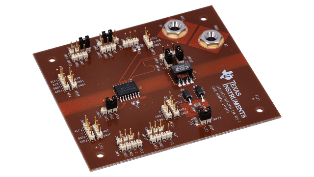
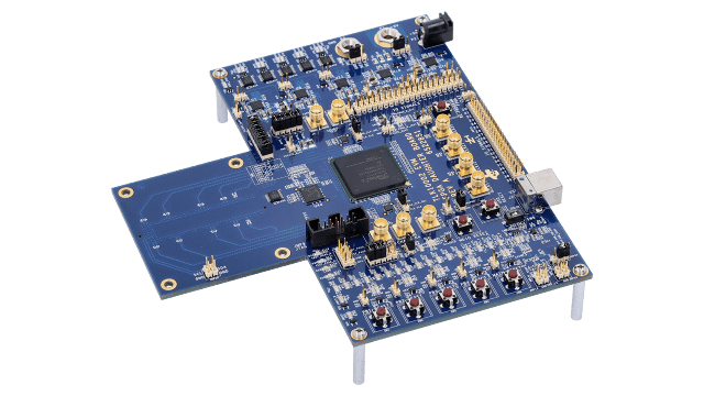
TPS2384EVM PoE Auto mode Evaluation Module
Texas Instruments
TPS2384EVM PoE Auto mode Evaluation Module
| Distributor | SKU | Stock | MOQ | 1 | 10 | 50 | 100 | 1,000 | 10,000 |
|---|---|---|---|---|---|---|---|---|---|
| DigiKey | 296-21150-ND | 0 | 1 | $319.22 | $319.22 | $319.22 | $319.22 | $319.22 | $319.22 |
| Arrow North American Components | TPS2384EVM | 0 | 1 | $246.19 | $243.73 | $238.88 | $236.49 | $229.46 | $151.28 |
| AVNET Europe | TPS2384EVM | 0 | 1 | * $191.72 | * $189.25 | * $184.55 | * $182.20 | * $182.20 | * $182.20 |
| AVNET Express | TPS2384EVM | 0 | 1 | $181.78 | $181.78 | $181.78 | $181.78 | $181.78 | $181.78 |
| Mouser Electronics | 595-TPS2384EVM | 0 | 1 | $197.19 | $197.19 | $197.19 | $197.19 | $197.19 | $197.19 |
| Texas Instruments | TPS2384EVM | 28 | 1 | $149.00 | $149.00 | $149.00 | $149.00 | $149.00 | $149.00 |
| Verical Marketplace | TPS2384EVM | 29 | 1 | $168.31 | $168.31 | $168.31 | $168.31 | $168.31 | $168.31 |
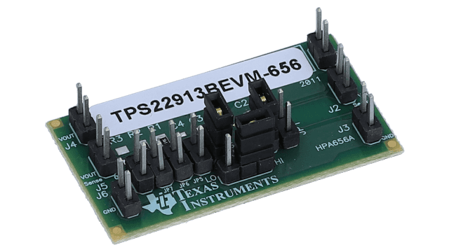
TPS22913B Ultra-Small, Low Ron, 2A Single-Channel Load Switch Evaluation Module
Texas Instruments
TPS22913B Ultra-Small, Low Ron, 2A Single-Channel Load Switch Evaluation Module
| Distributor | SKU | Stock | MOQ | 1 | 10 | 50 | 100 | 1,000 | 10,000 |
|---|---|---|---|---|---|---|---|---|---|
| DigiKey | 296-45899-ND | 0 | 1 | $31.25 | $31.25 | $31.25 | $31.25 | $31.25 | $31.25 |
| Arrow North American Components | TPS22913BEVM-656 | 0 | 1 | $31.19 | $29.90 | $29.90 | $29.32 | $28.93 | $28.93 |
| AVNET Express | TPS22913BEVM-656 | 0 | 1 | $30.50 | $30.50 | $30.50 | $30.50 | $30.50 | $30.50 |
| element14 APAC | TPS22913BEVM-656 | 6 | 1 | * $32.55 | * $32.55 | * $32.55 | * $32.55 | * $32.55 | * $32.55 |
| Farnell | TPS22913BEVM-656 | 6 | 1 | * $27.00 | * $27.00 | * $27.00 | * $27.00 | * $27.00 | * $27.00 |
| Mouser Electronics | 595-TPS22913BEVM-656 | 1 | 1 | $33.25 | $33.24 | $33.24 | $33.24 | $33.24 | $33.24 |
| Newark | TPS22913BEVM-656 | 0 | 1 | $25.89 | $25.89 | $25.89 | $25.89 | $25.89 | $25.89 |
| Texas Instruments | TPS22913BEVM-656 | 2 | 1 | $25.00 | $25.00 | $25.00 | $25.00 | $25.00 | $25.00 |
| Verical Marketplace | TPS22913BEVM-656 | 11 | 2 | $0.00 | $27.85 | $27.85 | $27.85 | $27.85 | $27.85 |
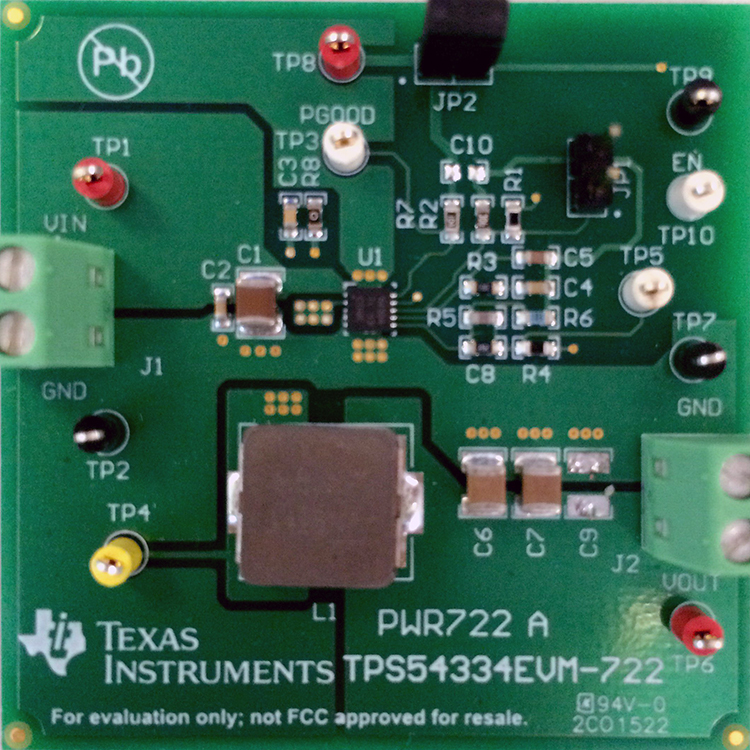
TPS54334EVM-722 3-A Regulator Evaluation Module
Texas Instruments
TPS54334EVM-722 3-A Regulator Evaluation Module
| Distributor | SKU | Stock | MOQ | 1 | 10 | 50 | 100 | 1,000 | 10,000 |
|---|---|---|---|---|---|---|---|---|---|
| DigiKey | 296-43195-ND | 1 | 1 | $61.25 | $61.25 | $61.25 | $61.25 | $61.25 | $61.25 |
| AVNET Europe | TPS54334EVM-722 | 0 | 1 | * $164.04 | * $172.02 | * $161.38 | * $156.06 | * $156.06 | * $156.06 |
| AVNET Express | TPS54334EVM-722 | 0 | 1 | $120.78 | $120.78 | $120.78 | $120.78 | $120.78 | $120.78 |
| Mouser Electronics | 595-TPS54334EVM-722 | 2 | 1 | $64.85 | $64.84 | $64.84 | $64.84 | $64.84 | $64.84 |
| Newark | TPS54334EVM-722 | 0 | $98.46 | $98.46 | $98.46 | $98.46 | $98.46 | $98.46 | |
| Texas Instruments | TPS54334EVM-722 | 23 | 1 | $49.00 | $49.00 | $49.00 | $49.00 | $49.00 | $49.00 |
300mA Linear Voltage Regulator for Digital Applications
Texas Instruments
300mA Linear Voltage Regulator for Digital Applications
| Distributor | SKU | Stock | MOQ | 1 | 10 | 50 | 100 | 1,000 | 10,000 |
|---|---|---|---|---|---|---|---|---|---|
| DigiKey | LP3991TL-1.8EV-ND | 1 | 1 | $26.40 | $26.40 | $26.40 | $26.40 | $26.40 | $26.40 |
| Arrow North American Components | LP3991TL-1.8EV | 0 | 1 | $0.00 | $25.93 | $25.93 | $25.71 | $25.58 | $25.58 |
| AVNET Express | LP3991TL-1.8EV | 0 | 1 | $0.00 | $0.00 | $0.00 | $0.00 | $0.00 | $0.00 |
| element14 APAC | LP3991TL-1.8EV | 0 | 1 | * $32.51 | * $32.51 | * $32.51 | * $32.51 | * $32.51 | * $32.51 |
| Farnell | LP3991TL-1.8EV | 0 | 1 | * $36.46 | * $36.46 | * $36.46 | * $36.46 | * $36.46 | * $36.46 |
| Mouser Electronics | 926-LP3991TL-1.8EV | 0 | 1 | $0.00 | |||||
| Newark | LP3991TL-1.8EV | 0 | 1 | $25.89 | $25.89 | $25.89 | $25.89 | $25.89 | $25.89 |
| Texas Instruments | LP3991TL-1.8EV | 6 | 1 | $25.00 | $25.00 | $25.00 | $25.00 | $25.00 | $25.00 |
| Verical Marketplace | LP3991TL-1.8EV | 5 | 2 | $29.31 | $29.31 | $29.31 | $29.31 | $29.31 |
| Distributor | SKU | Stock | MOQ | 1 | 10 | 50 | 100 | 1,000 | 10,000 |
|---|---|---|---|---|---|---|---|---|---|
| DigiKey | 296-50048-ND | 0 | 1 | $53.90 | $53.90 | $53.90 | $53.90 | $53.90 | $53.90 |
| Arrow North American Components | TPS2044BEVM-295 | 0 | 1 | $0.00 | $62.11 | $62.11 | $55.07 | $52.26 | $52.26 |
| AVNET Express | TPS2044BEVM-295 | 0 | 1 | $0.00 | $0.00 | $0.00 | $0.00 | $0.00 | $0.00 |
| Mouser Electronics | 595-TPS2044BEVM-295 | 0 | 1 | $0.00 | |||||
| Texas Instruments | TPS2044BEVM-295 | 8 | 1 | $49.00 | $49.00 | $49.00 | $49.00 | $49.00 | $49.00 |
| Win Source | TPS2044BEVM-295 | 4 | 1 |
| Distributor | SKU | Stock | MOQ | 1 | 10 | 50 | 100 | 1,000 | 10,000 |
|---|---|---|---|---|---|---|---|---|---|
| DigiKey | ADS6224EVM-ND | 0 | 1 | $0.00 | $0.00 | $0.00 | $0.00 | $0.00 | $0.00 |
| Mouser Electronics | 595-ADS6224EVM | 0 | 1 | ||||||
| Texas Instruments | ADS6224EVM | 3 | 1 | $299.00 | $299.00 | $299.00 | $299.00 | $299.00 | $299.00 |
Evaluation Module for Single-Chip Charger and DC/DC Converter IC for Portable Applications
Texas Instruments
Evaluation Module for Single-Chip Charger and DC/DC Converter IC for Portable Applications
| Distributor | SKU | Stock | MOQ | 1 | 10 | 50 | 100 | 1,000 | 10,000 |
|---|---|---|---|---|---|---|---|---|---|
| DigiKey | BQ25017EVM-ND | 0 | 1 | $0.00 | $0.00 | $0.00 | $0.00 | $0.00 | $0.00 |
| AVNET Express | BQ25017EVM | 0 | 1 | $0.00 | $0.00 | $0.00 | $0.00 | $0.00 | $0.00 |
| Mouser Electronics | 595-BQ25017EVM | 0 | 1 | ||||||
| Texas Instruments | BQ25017EVM | 18 | $49.00 |
| Distributor | SKU | Stock | MOQ | 1 | 10 | 50 | 100 | 1,000 | 10,000 |
|---|---|---|---|---|---|---|---|---|---|
| DigiKey | 296-31025-ND | 1 | 1 | $3,598.80 | $3,598.80 | $3,598.80 | $3,598.80 | $3,598.80 | $3,598.80 |
| Arrow North American Components | TLK10002FPGAEVM | 0 | 1 | $3,460.38 | $0.00 | $0.00 | $0.00 | $0.00 | $0.00 |
| AVNET Express | TLK10002FPGAEVM | 0 | 1 | $3,658.78 | $3,658.78 | $3,658.78 | $3,658.78 | $3,658.78 | $3,658.78 |
| element14 APAC | TLK10002FPGAEVM | 0 | 1 | * $3,782.70 | * $3,782.70 | * $3,782.70 | * $3,782.70 | * $3,782.70 | * $3,782.70 |
| Farnell | TLK10002FPGAEVM | 0 | 1 | * $3,617.70 | * $3,617.70 | * $3,617.70 | * $3,617.70 | * $3,617.70 | * $3,617.70 |
| Mouser Electronics | 595-TLK10002FPGAEVM | 1 | 1 | $3,969.02 | $3,969.02 | $3,969.02 | $3,969.02 | $3,969.02 | $3,969.02 |
| Newark | TLK10002FPGAEVM | 1 | 1 | $3,298.90 | $3,298.90 | $3,298.90 | $3,298.90 | $3,298.90 | $3,298.90 |
| Texas Instruments | TLK10002FPGAEVM | 6 | 1 | $2,999.00 | $2,999.00 | $2,999.00 | $2,999.00 | $2,999.00 | $2,999.00 |
| Verical Marketplace | TLK10002FPGAEVM | 3 | 1 | $3,341.13 | $3,341.13 | $3,341.13 | $3,341.13 | $3,341.13 | $3,341.13 |
| Win Source | TLK10002FPGAEVM | 2 | 1 |
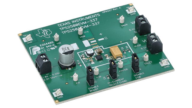
Power-Distribution Switch with Low Voltage Input Evaluation Module for TPS2500
Texas Instruments
Power-Distribution Switch with Low Voltage Input Evaluation Module for TPS2500
| Distributor | SKU | Stock | MOQ | 1 | 10 | 50 | 100 | 1,000 | 10,000 |
|---|---|---|---|---|---|---|---|---|---|
| DigiKey | 296-31142-ND | 6 | 1 | $58.80 | $58.80 | $58.80 | $58.80 | $58.80 | $58.80 |
| AVNET Express | TPS2500EVM-337 | 0 | 1 | $59.78 | $59.78 | $59.78 | $59.78 | $59.78 | $59.78 |
| element14 APAC | TPS2500EVM-337 | 0 | 1 | * $60.05 | * $60.05 | * $60.05 | * $60.05 | * $60.05 | * $60.05 |
| Farnell | TPS2500EVM-337 | 0 | 1 | * $65.82 | * $65.82 | * $65.82 | * $65.82 | * $65.82 | * $65.82 |
| Mouser Electronics | 595-TPS2500EVM-337 | 3 | 1 | $64.85 | $64.84 | $64.84 | $64.84 | $64.84 | $64.84 |
| Newark | TPS2500EVM-337 | 0 | 1 | $50.73 | $50.73 | $50.73 | $50.73 | $50.73 | $50.73 |
| Texas Instruments | TPS2500EVM-337 | 16 | 1 | $49.00 | $49.00 | $49.00 | $49.00 | $49.00 | $49.00 |