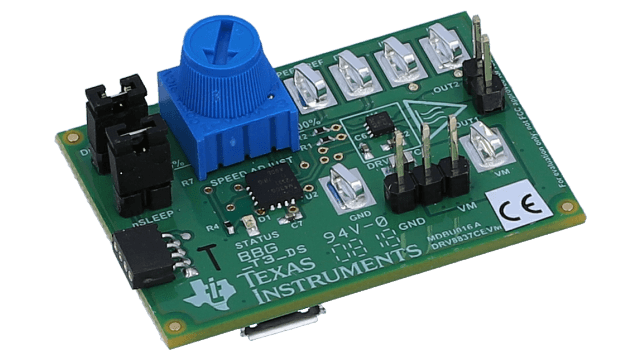
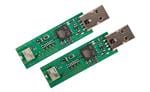
1-A Low-Voltage H-Bridge Evaluation Module
Texas Instruments
1-A Low-Voltage H-Bridge Evaluation Module
| Distributor | SKU | Stock | MOQ | 1 | 10 | 50 | 100 | 1,000 | 10,000 |
|---|---|---|---|---|---|---|---|---|---|
| DigiKey | 296-46704-ND | 2 | 1 | $58.80 | $58.80 | $58.80 | $58.80 | $58.80 | $58.80 |
| Arrow North American Components | DRV8837CEVM | 1 | 1 | $57.57 | $57.57 | $57.57 | $57.57 | $57.57 | $57.57 |
| AVNET Express | DRV8837CEVM | 0 | 1 | $59.78 | $59.78 | $59.78 | $59.78 | $59.78 | $59.78 |
| Mouser Electronics | 595-DRV8837CEVM | 0 | 1 | $64.85 | $64.85 | $64.85 | $64.85 | $64.85 | $64.85 |
| Newark | DRV8837CEVM | 0 | 1 | $50.73 | $50.73 | $50.73 | $50.73 | $50.73 | $50.73 |
| Texas Instruments | DRV8837CEVM | 28 | 1 | $49.00 | $49.00 | $49.00 | $49.00 | $49.00 | $49.00 |
| Verical Marketplace | DRV8837CEVM | 1 | 1 | $57.57 | $57.57 | $57.57 | $57.57 | $57.57 | $57.57 |
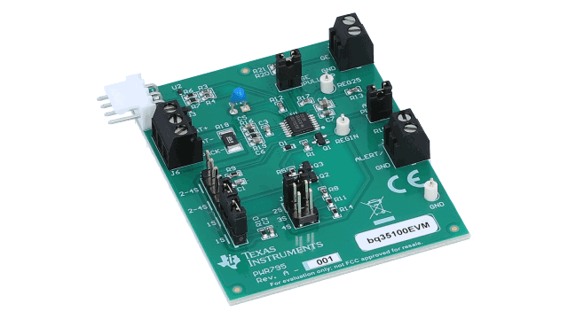
bq35100 Lithium Primary Cell Evaluation Module Using End-of-Service Monitor Gas Gauging
Texas Instruments
bq35100 Lithium Primary Cell Evaluation Module Using End-of-Service Monitor Gas Gauging
| Distributor | SKU | Stock | MOQ | 1 | 10 | 50 | 100 | 1,000 | 10,000 |
|---|---|---|---|---|---|---|---|---|---|
| DigiKey | 296-45216-ND | 17 | 1 | $96.00 | $96.00 | $96.00 | $96.00 | $96.00 | $96.00 |
| Arrow North American Components | BQ35100EVM-795 | 1 | 1 | $51.36 | $51.36 | $51.36 | $51.36 | $51.36 | $51.36 |
| AVNET Europe | BQ35100EVM-795 | 0 | 1 | * $140.64 | * $136.51 | * $128.84 | * $125.18 | * $125.18 | * $125.18 |
| AVNET Express | BQ35100EVM-795 | 0 | 1 | $120.78 | $120.78 | $120.78 | $120.78 | $120.78 | $120.78 |
| element14 APAC | BQ35100EVM-795 | 0 | 1 | * $114.18 | * $114.18 | * $114.18 | * $114.18 | * $114.18 | * $114.18 |
| Farnell | BQ35100EVM-795 | 0 | 1 | * $108.89 | * $108.89 | * $108.89 | * $108.89 | * $108.89 | * $108.89 |
| Mouser Electronics | 595-BQ35100EVM-795 | 14 | 1 | $118.81 | $118.81 | $118.81 | $118.81 | $118.81 | $118.81 |
| Newark | BQ35100EVM-795 | 0 | 1 | $102.50 | $102.50 | $102.50 | $102.50 | $102.50 | $102.50 |
| Texas Instruments | BQ35100EVM-795 | 30 | 1 | $80.00 | $80.00 | $80.00 | $80.00 | $80.00 | $80.00 |
| Verical Marketplace | BQ35100EVM-795 | 1 | 1 | $51.36 | $0.00 | $0.00 | $0.00 | $0.00 | $0.00 |
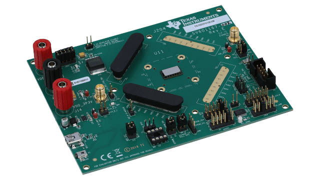
28 Gbps multi-rate 8-channel retimer evaluation module
Texas Instruments
28 Gbps multi-rate 8-channel retimer evaluation module
| Distributor | SKU | Stock | MOQ | 1 | 10 | 50 | 100 | 1,000 | 10,000 |
|---|---|---|---|---|---|---|---|---|---|
| DigiKey | 296-DS280DF810EVM-ND | 2 | 1 | $1,798.80 | $1,798.80 | $1,798.80 | $1,798.80 | $1,798.80 | $1,798.80 |
| Arrow North American Components | DS280DF810EVM | 0 | 1 | $2,068.94 | $2,048.25 | $2,007.49 | $1,987.42 | $1,917.80 | $1,898.62 |
| AVNET Express | DS280DF810EVM | 0 | 1 | $1,828.78 | $1,828.78 | $1,828.78 | $1,828.78 | $1,828.78 | $1,828.78 |
| Mouser Electronics | 595-DS280DF810EVM | 0 | 1 | $1,983.85 | $1,983.85 | $1,983.85 | $1,983.85 | $1,983.85 | $1,983.85 |
| Texas Instruments | DS280DF810EVM | 10 | 1 | $1,499.00 | $1,499.00 | $1,499.00 | $1,499.00 | $1,499.00 | $1,499.00 |
| Verical Marketplace | DS280DF810EVM | 36 | 1 | $1,798.66 | $1,798.66 | $1,798.66 | $1,798.66 | $1,798.66 | $1,798.66 |
EVAL_PAN1322
Panasonic Industrial Devices
Evaluation Board for PAN1322 Bluetooth Module BT2.1 Class 2 Application w/Ant.
| Distributor | SKU | Stock | MOQ | 1 | 10 | 50 | 100 | 1,000 | 10,000 |
|---|---|---|---|---|---|---|---|---|---|
| DigiKey | P16275-ND | 0 | 10 | $0.00 | $0.00 | $0.00 | $0.00 | $0.00 | |
| Future Electronics | EVAL_PAN1322 | 6 | $124.00 | ||||||
| Mouser Electronics | 667-EVAL_PAN1322 | 0 | 1 |
EVAL_PAN1740
Panasonic Industrial Devices
Evaluation kit for BLE Bluetooth Low Energy Module Dialog DA14580
| Distributor | SKU | Stock | MOQ | 1 | 10 | 50 | 100 | 1,000 | 10,000 |
|---|---|---|---|---|---|---|---|---|---|
| DigiKey | P18969-ND | 7 | 1 | $17.56 | $21.57 | $19.86 | $19.86 | $15.32 | $15.32 |
| Future Electronics | EVAL_PAN1740 | 39 | $130.00 | ||||||
| Mouser Electronics | 667-EVAL_PAN1740 | 23 | 1 | $143.61 | $143.61 | $143.61 | $143.61 | $143.61 | $143.61 |
| Distributor | SKU | Stock | MOQ | 1 | 10 | 50 | 100 | 1,000 | 10,000 |
|---|---|---|---|---|---|---|---|---|---|
| DigiKey | 497-13000-ND | 1 | 1 | $65.21 | $65.21 | $65.21 | $65.21 | $65.21 | $65.21 |
| Ameya360 | EVAL6393FB | 2 | $79.33 | $79.33 | $79.33 | $79.33 | $79.33 | $79.33 | |
| Arrow North American Components | EVAL6393FB | 0 | 1 | $48.92 | $48.92 | $48.92 | $48.92 | $48.92 | $48.92 |
| AVNET Express | EVAL6393FB | 0 | 1 | $0.00 | $0.00 | $0.00 | $0.00 | $0.00 | |
| element14 APAC | EVAL6393FB | 9 | 1 | * $89.38 | * $89.37 | * $89.37 | * $89.37 | * $89.37 | * $89.37 |
| Farnell | EVAL6393FB | 9 | 1 | * $0.00 | * $0.00 | * $68.09 | * $68.09 | * $68.09 | * $68.09 |
| Future Electronics | EVAL6393FB | 1 | 1 | $72.12 | $61.48 | $61.48 | $61.48 | $61.48 | $61.48 |
| Mouser Electronics | 511-EVAL6393FB | 5 | 1 | $66.25 | $66.25 | $66.25 | $66.25 | $66.25 | $66.25 |
| Newark | EVAL6393FB | 1 | 9 | $0.00 | $0.00 | $0.00 | $0.00 | $0.00 | $0.00 |
| Verical Marketplace | EVAL6393FB | 6 | 1 | $48.92 | $48.92 | $48.92 | $48.92 | $48.92 | $48.92 |
| Win Source | EVAL6393FB | 480 | 1 |
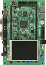
STM32100E-EVAL
STMicroelectronics
Evaluation Board for ARM Cortex-M3 Core-based STM32F100 Microcontroller
| Distributor | SKU | Stock | MOQ | 1 | 10 | 50 | 100 | 1,000 | 10,000 |
|---|---|---|---|---|---|---|---|---|---|
| DigiKey | 497-12897-ND | 0 | 1 | $286.25 | $286.25 | $286.25 | $286.25 | $286.25 | $286.25 |
| Ameya360 | STM32100E-EVAL | 1 | $317.90 | $317.90 | $317.90 | $317.90 | $317.90 | $317.90 | |
| AVNET Europe | STM32100E-EVAL | 2 | 1 | * $0.00 | * $0.00 | * $0.00 | * $0.00 | * $0.00 | * $0.00 |
| AVNET Express | STM32100E-EVAL | 0 | 1 | $0.00 | $0.00 | $0.00 | $0.00 | $0.00 | |
| element14 APAC | STM32100E-EVAL | 0 | 1 | * $314.80 | * $314.80 | * $314.80 | * $314.80 | * $314.80 | * $314.80 |
| Farnell | STM32100E-EVAL | 0 | 1 | * $303.45 | * $303.45 | * $303.45 | * $303.45 | * $303.45 | * $303.45 |
| Future Electronics | STM32100E-EVAL | 1 | 1 | $289.00 | $289.00 | $289.00 | $289.00 | $289.00 | $289.00 |
| Mouser Electronics | 511-STM32100E-EVAL | 1 | 1 | $297.72 | $297.72 | $297.72 | $297.72 | $297.72 | $297.72 |
| Newark | STM32100E-EVAL | 0 | 3 | $0.00 | $0.00 | $0.00 | $0.00 | $0.00 | $0.00 |
| RS Components | STM32100E-EVAL | 0 | $258.37 |
| Distributor | SKU | Stock | MOQ | 1 | 10 | 50 | 100 | 1,000 | 10,000 |
|---|---|---|---|---|---|---|---|---|---|
| DigiKey | ISL8026EVAL3Z-ND | 0 | $66.25 | $66.25 | $66.25 | $66.25 | $66.25 | $66.25 | |
| Ameya360 | ISL8026EVAL3Z | 2 | $85.11 | $85.11 | $85.11 | $85.11 | $85.11 | $85.11 | |
| AVNET Express | ISL8026EVAL3Z | 1 | 1 | $0.00 | $0.00 | $0.00 | $0.00 | $0.00 | $0.00 |
| Future Electronics | ISL8026EVAL3Z | 2 | 1 | $71.42 | $61.15 | $61.15 | $61.15 | $61.15 | $61.15 |
| Mouser Electronics | N/A | 0 | $0.00 | ||||||
| RS Components | ISL8026EVAL3Z | 0 | $59.18 | ||||||
| RS Components (APAC) | ISL8026EVAL3Z | 0 | $111.31 | ||||||
| Rutronik | ISL8026EVAL3Z | 2 | 1 | $69.92 |
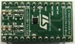
STEVAL-MKI163V1
STMicroelectronics
LSM303C 3 Axis Sensor Adapter Evaluation Board for Standard DIL24 Socket
| Distributor | SKU | Stock | MOQ | 1 | 10 | 50 | 100 | 1,000 | 10,000 |
|---|---|---|---|---|---|---|---|---|---|
| DigiKey | 497-15394-ND | 0 | 1 | $17.81 | $17.81 | $17.81 | $17.81 | $17.81 | $17.81 |
| AVNET Asia Pacific | STEVAL-MKI163V1 | 0 | 1 | $0.00 | $0.00 | $0.00 | $0.00 | $0.00 | $0.00 |
| AVNET Express | STEVAL-MKI163V1 | 0 | 1 | $17.09 | $16.98 | $16.07 | $16.07 | ||
| element14 APAC | STEVAL-MKI163V1 | 1 | 1 | * $24.49 | * $24.49 | * $24.49 | * $24.49 | * $24.49 | * $24.49 |
| Farnell | STEVAL-MKI163V1 | 1 | 1 | * $16.43 | * $16.43 | * $16.43 | * $16.43 | * $16.43 | * $16.43 |
| Future Electronics | STEVAL-MKI163V1 | 4 | 1 | $15.88 | $15.88 | $15.88 | $15.88 | $15.88 | $15.88 |
| Mouser Electronics | 511-STEVAL-MKI163V1 | 0 | 1 | $0.00 | |||||
| Newark | STEVAL-MKI163V1 | 1 | 1 | $17.96 | $17.96 | $17.96 | $17.96 | $17.96 | $17.96 |
| RS Components | STEVAL-MKI163V1 | 0 | $16.38 | ||||||
| RS Components (APAC) | STEVAL-MKI163V1 | 0 | $36.63 | ||||||
| Rutronik | STEVAL-MKI163V1 | 0 | 1 | $32.31 | |||||
| Win Source | STEVAL-MKI163V1 | 2600 |
| Distributor | SKU | Stock | MOQ | 1 | 10 | 50 | 100 | 1,000 | 10,000 |
|---|---|---|---|---|---|---|---|---|---|
| DigiKey | 497-15206-ND | 0 | 1 | $32.45 | $32.45 | $32.45 | $32.45 | $32.45 | $32.45 |
| Ameya360 | STEVAL-SP1ML915 | 0 | $38.23 | $38.23 | $38.23 | $38.23 | $38.23 | $38.23 | |
| Arrow North American Components | STEVAL-SP1ML915 | 0 | 20 | $43.32 | $42.89 | $43.56 | $43.13 | $41.85 | $40.60 |
| AVNET Europe | STEVAL-SP1ML915 | 1 | 1 | * $0.00 | * $0.00 | * $0.00 | * $0.00 | * $0.00 | * $0.00 |
| AVNET Express | STEVAL-SP1ML915 | 0 | 1 | $0.00 | $0.00 | $0.00 | $0.00 | ||
| element14 APAC | STEVAL-SP1ML915 | 1 | 1 | * $39.18 | * $39.18 | * $39.18 | * $39.18 | * $39.18 | * $39.18 |
| Farnell | STEVAL-SP1ML915 | 1 | 1 | * $33.14 | * $33.14 | * $33.14 | * $33.14 | * $33.14 | * $33.14 |
| Future Electronics | STEVAL-SP1ML915 | 3 | 1 | $32.05 | $32.05 | $32.05 | $32.05 | $32.05 | $32.05 |
| Mouser Electronics | 511-STEVAL-SP1ML915 | 0 | 1 | $0.00 | |||||
| Newark | STEVAL-SP1ML915 | 0 | 20 | $0.00 | $0.00 | $0.00 | $0.00 | $0.00 | $0.00 |
| RS Components | STEVAL-SP1ML915 | 0 | $24.46 | ||||||
| Verical Marketplace | STEVAL-SP1ML915 | 1 | 1 | $29.62 | $29.62 | $29.62 | $29.62 | $29.62 | $29.62 |