
ADRV9008-2W/PCBZ
Analog Devices Inc.
The ADRV9008-2 is a highly integrated, RF agile transmit subsystem offering dual channel transmitters, observation path receiver, integrated synthesizers, and digital signal processing functions. The IC delivers a versatile combination of high performance and low power consumption demanded by 2G, 3G and 4G macro-cell base stations, and active antenna, applications.The transmitters use an innovative direct conversion modulator that achieves multi-carrier macro-base-station quality performance and very low power. In 3G/4G mode, the maximum large-signal bandwidth is 200MHz. In MC-GSM mode, which has higher in-band SFDR, the maximum large-signal bandwidth is 75MHz.The observation path consists of a wide bandwidth direct-conversion receiver with state-of-the-art dynamic range. The complete receive subsystem includes dc offset correction, quadrature correction, and digital filtering thus eliminating the need for these functions in the digital baseband. Several auxiliary functions such as ADCs, DACs, and GPIOs for PA and RF-front-end control are also integrated. The fully integrated phase locked loops (PLLs) provide high performance, low power fractional-N RF frequency synthesis for the transmitter and receiver sections. An additional synthesizer is used to generate the clocks needed for the converters, digital circuits, and the serial interface. Special precautions have been taken to provide the isolation demanded in high performance base station applications. All VCO and loop filter components are integrated.The high-speed JESD204B interface supports up to 12.288 Gbps lane rates resulting in two lanes per transmitter in the widest bandwidth mode and two lanes for the observation path receiver in the widest bandwidth mode. The core of the ADRV9008-2 can be powered directly from 1.3 V and 1.8 V regulators and is controlled via a standard 4 wire serial port. Comprehensive power-down modes are included to minimize power consumption in normal use. The ADRV9008-2 is packaged in a 12mm ? 12 mm, 196-ball chip scale ball grid array (CSP_BGA).
| Distributor | SKU | Stock | MOQ | 1 | 10 | 50 | 100 | 1,000 | 10,000 |
|---|---|---|---|---|---|---|---|---|---|
| Analog Devices Inc | ADRV9008-2W/PCBZ | 0 | $1,317.38 | $1,317.38 | $1,317.38 | $1,317.38 | $1,317.38 | $1,317.38 | |
| Mouser Electronics | 584-ADRV9008-2W/PCBZ | 1 | 1 | $1,420.17 | $1,420.17 | $1,420.17 | $1,420.17 | $1,420.17 | $1,420.17 |

ADRV9009-W/PCBZ
Analog Devices Inc.
The ADRV9009 is a highly integrated, radio frequency (RF), agile transceiver offering dual transmitters and receivers, integrated synthesizers, and digital signal processing functions. The IC delivers a versatile combination of high performance and low power consumption demanded by 3G, 4G, and 5G macro cell time division duplex (TDD) base station applications.The receive path consists of two independent, wide bandwidth, direct conversion receivers with state-of-the-art dynamic range. The device also supports a wide bandwidth, time shared observation path receiver (ORx) for use in TDD applications. The complete receive subsystem includes automatic and manual attenuation control, dc offset correction, quadrature error correction (QEC), and digital filtering, thus eliminating the need?for these functions in the digital baseband. Several auxiliary functions, such as analog-to-digital converters (ADCs), digital-to-analog converters (DACs), and general-purpose inputs/outputs (GPIOs) for the power amplifier (PA), and RF front-end control are also integrated.In addition to automatic gain control (AGC), the ADRV9009 also features flexible external gain control modes, allowing significant flexibility in setting system level gain dynamically.The received signals are digitized with a set of four high dynamic range, continuous time ?-? ADCs that provide inherent antialiasing. The combination of the direct conversion architecture, which does not suffer from out of band image mixing, and the lack of aliasing, relaxes the requirements of the RF filters when compared to traditional intermediate frequency (IF) receivers.The transmitters use an innovative direct conversion modulator that achieves high modulation accuracy with exceptionally low noise.The observation receiver path consists of a wide bandwidth, direct conversion receiver with state-of-the-art dynamic range.The fully integrated phase-locked loop (PLL) provides high performance, low power, fractional-N RF frequency synthesis for the transmitter (Tx) and receiver (Rx) signal paths. An additional synthesizer generates the clocks needed for the converters, digital circuits, and the serial interface. A multichip synchronization mechanism synchronizes the phase of the RF local oscillator (LO) and baseband clocks between multiple ADRV9009 chips. Precautions are taken to provide the isolation required in high performance base station applications. All voltage controlled oscillators (VCOs) and loop filter components are integrated.The high speed JESD204B interface supports up to 12.288 Gbps lane rates, resulting in two lanes per transmitter and a single lane per receiver in the widest bandwidth mode. The interface also supports interleaved mode for lower bandwidths, thus reducing the total number of high speed data interface lanes to one. Both fixed and floating point data formats are supported. The floating point format allows internal AGC to be invisible to the demodulator device.The core of the ADRV9009 can be powered directly from 1.3 V regulators and 1.8 V regulators, and is controlled via a standard 4-wire serial port. Comprehensive power-down modes are included to minimize power consumption in normal use. The ADRV9009 is packaged in a 12 mm ? 12 mm, 196-ball chip scale ball grid array (CSP_BGA).Applications 3G, 4G, and 5G TDD macrocell base stations TDD active antenna systems Massive multiple input, multiple output (MIMO) Phased array radar Electronic warfare Military communications Portable test equipment
| Distributor | SKU | Stock | MOQ | 1 | 10 | 50 | 100 | 1,000 | 10,000 |
|---|---|---|---|---|---|---|---|---|---|
| Analog Devices Inc | ADRV9009-W/PCBZ | 0 | $2,010.74 | $2,010.74 | $2,010.74 | $2,010.74 | $2,010.74 | $2,010.74 | |
| element14 APAC | ADRV9009-W/PCBZ | 2 | 1 | * $2,185.22 | * $2,185.22 | * $2,185.22 | * $2,185.22 | * $2,185.22 | * $2,185.22 |
| Farnell | ADRV9009-W/PCBZ | 4 | 1 | * $2,120.79 | * $2,120.79 | * $2,120.79 | * $2,120.79 | * $2,120.79 | * $2,120.79 |
| Mouser Electronics | 584-ADRV9009-W/PCBZ | 4 | 1 | $2,167.64 | $2,167.64 | $2,167.64 | $2,167.64 | $2,167.64 | $2,167.64 |
| Newark | ADRV9009-W/PCBZ | 2 | 1 | $2,151.42 | $2,151.42 | $2,151.42 | $2,151.42 | $2,151.42 | $2,151.42 |
| Win Source | ADRV9009-W/PCBZ | 1 | 1 |

ADRV9029-LB/PCBZ
Analog Devices Inc.
The ADRV9029 is a highly integrated, radio frequency (RF) agile transceiver offering four independently controlled transmitters, dedicated observation receiver inputs for monitoring each transmitter channel, four independently controlled receivers, integrated synthesizers, and digital signal processing functions providing a complete transceiver solution. The device provides the performance demanded by cellular infrastructure applications, such as small cell base station radios, macro 3G/4G/5G systems, and massive multiple in/multiple out (MIMO) base stations.The receiver subsystem consists of four independent, wide bandwidth, direct conversion receivers with wide dynamic range. The four independent transmitters use a direct conversion modulator resulting in low noise operation with low power consumption. The device also includes two wide bandwidth, time shared, observation path receivers with two inputs each for monitoring transmitter outputs.The complete transceiver subsystem includes automatic and manual attenuation control, dc offset correction, quadrature error correction (QEC), and digital filtering, eliminating the need for these functions in the digital baseband. Other auxiliary functions such as analog-to-digital converters (ADCs), digital-to-analog converters (DACs), and general-purpose input/ outputs (GPIOs) that provide an array of digital control options are also integrated.To achieve a high level of RF performance, the transceiver includes five fully integrated phase-locked loops (PLLs). Two PLLs provide low noise and low power fractional-N RF synthesis for the transmitter and receiver signal paths. A third fully integrated PLL supports an independent local oscillator (LO) mode for the observation receiver. The fourth PLL generates the clocks needed for the converters and digital circuits, and a fifth PLL provides the clock for the serial data interface.A multichip synchronization mechanism synchronizes the phase of all LOs and baseband clocks between multiple ADRV9029 chips. All voltage controlled oscillators (VCOs) and loop filter components are integrated and adjustable through the digital control interface.This device contains a fully integrated, low power digital predistortion (DPD) adaptation engine for use in power amplifier linearization. DPD enables use of high efficiency power amplifiers, reducing the power consumption of base station radios while also reducing the number of SERDES lanes necessary to interface with baseband processors.The low power crest factor reduction (CFR) engine of the ADRV9029 reduces the peak to average ratio (PAR) of the input signal, enabling higher efficiency transmit line ups while reducing the processing load on baseband processors.The serial data interface consists of four serializer lanes and four deserializer lanes. The interface supports both the JESD204B and JESD204C standards, operating at data rates up to 24.33 Gbps. The interface also supports interleaved mode for lower bandwidths, thus reducing the number of high speed data interface lanes to one. Both fixed and floating-point data formats are supported. The floating-point format allows internal automatic gain control (AGC) to be invisible to the demodulator device.The ADRV9029 is powered directly from 1.0 V, 1.3 V, and 1.8 V regulators and is controlled via a standard serial peripheral interface (SPI) serial port. Comprehensive power-down modes are included to minimize power consumption in normal use. The ADRV9029 is packaged in a 14 mm ? 14 mm, 289-ball chip scale ball grid array (CSP_BGA).APPLICATIONS3G/4G/5G TDD and FDD massive MIMO, macro and small cell base stations
| Distributor | SKU | Stock | MOQ | 1 | 10 | 50 | 100 | 1,000 | 10,000 |
|---|---|---|---|---|---|---|---|---|---|
| Mouser Electronics | N/A | 0 |

LT3080EDD Demo Board | LT3080(x4), Paralleled, Single Resistor LDOs, 3.8V ≤ VIN ≤ 25V, VOUT = 3.3V @ 4.4A
Analog Devices Inc.
LT3080. A small 20 mΩ ballast resistor is required for parallel operation. A short PCB trace can easily
| Distributor | SKU | Stock | MOQ | 1 | 10 | 50 | 100 | 1,000 | 10,000 |
|---|---|---|---|---|---|---|---|---|---|
| Analog Devices Inc | DC1294A | 0 | $105.92 | $105.92 | $105.92 | $105.92 | $105.92 | $105.92 | |
| Mouser Electronics | 584-DC1294A | 5 | 1 | $109.62 | $109.62 | $109.62 | $109.62 | $109.62 | $109.62 |

EVAL-ADT7422MBZ
Analog Devices Inc.
need?for calibration after the PCB soldering process.Operating at 3.0 V, the average supply current
| Distributor | SKU | Stock | MOQ | 1 | 10 | 50 | 100 | 1,000 | 10,000 |
|---|---|---|---|---|---|---|---|---|---|
| Analog Devices Inc | EVAL-ADT7422MBZ | 0 | $24.55 | $24.55 | $24.55 | $24.55 | $24.55 | $24.55 | |
| element14 APAC | EVAL-ADT7422MBZ | 11 | 1 | * $24.81 | * $24.81 | * $24.81 | * $24.81 | * $24.81 | * $24.81 |
| Farnell | EVAL-ADT7422MBZ | 10 | 1 | * $24.11 | * $24.11 | * $24.11 | * $24.11 | * $24.11 | * $24.11 |
| Mouser Electronics | 584-EVAL-ADT7422MBZ | 102 | 1 | $23.88 | $23.88 | $23.88 | $23.88 | $23.88 | $23.88 |
| Newark | EVAL-ADT7422MBZ | 17 | 1 | $24.41 | $24.41 | $24.41 | $24.41 | $24.41 | $24.41 |

EV-ADF4196SD1Z
Analog Devices Inc.
This decreases the cost, complexity, PCB area, shielding, and characterization found on previous
| Distributor | SKU | Stock | MOQ | 1 | 10 | 50 | 100 | 1,000 | 10,000 |
|---|---|---|---|---|---|---|---|---|---|
| Mouser Electronics | N/A | 0 |

3.3V VIN, Dual 2A, 6MHz Synchronous Step-Down Regulators at 1.8V and 2.0V Outputs, in a 0.71cm2 Solution
Analog Devices Inc.
The PCB Considerations section in the data sheet.
The Efficiency vs Load graph on the demo manual
| Distributor | SKU | Stock | MOQ | 1 | 10 | 50 | 100 | 1,000 | 10,000 |
|---|---|---|---|---|---|---|---|---|---|
| Analog Devices Inc | DC2748A | 0 | $100.05 | $100.05 | $100.05 | $100.05 | $100.05 | $100.05 | |
| element14 APAC | DC2748A | 2 | 1 | * $111.96 | * $111.96 | * $111.96 | * $111.96 | * $111.96 | * $111.96 |
| Farnell | DC2748A | 2 | 1 | * $111.84 | * $111.84 | * $111.84 | * $111.84 | * $111.84 | * $111.84 |
| Mouser Electronics | 584-DC2748A | 0 | 1 | $103.54 | $103.54 | $103.54 | $103.54 | $103.54 | $103.54 |
| Newark | DC2748A | 2 | 1 | $102.50 | $102.50 | $102.50 | $102.50 | $102.50 | $102.50 |

LT8644S | 8V, 16A Synchronous Step-Down Silent Switcher 2
Analog Devices Inc.
EMI PCB Layout and Thermal Considerations. Contact ADI applications engineer for support.
| Distributor | SKU | Stock | MOQ | 1 | 10 | 50 | 100 | 1,000 | 10,000 |
|---|---|---|---|---|---|---|---|---|---|
| Analog Devices Inc | DC2779A | 0 | $107.00 | $107.00 | $107.00 | $107.00 | $107.00 | $107.00 | |
| Mouser Electronics | 584-DC2779A | 3 | 1 | $110.73 | $110.73 | $110.73 | $110.73 | $110.73 | $110.73 |
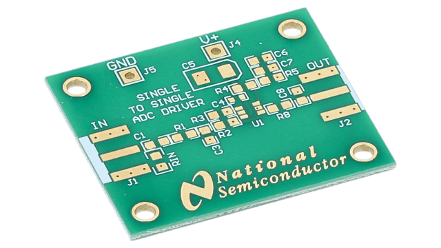
Single to Single ADC Driver PCB for LMH6611 and LMH6618 (SOT23 package; unstuffed)
Texas Instruments
Single to Single ADC Driver PCB for LMH6611 and LMH6618 (SOT23 package; unstuffed)
| Distributor | SKU | Stock | MOQ | 1 | 10 | 50 | 100 | 1,000 | 10,000 |
|---|---|---|---|---|---|---|---|---|---|
| Digi-Key | 551600083-001/NOPB-ND | 3 | 1 | $6.00 | $6.00 | $6.00 | $6.00 | $6.00 | $6.00 |

EVAL-LTC6229MS8E
Analog Devices Inc.
supply operation.For space constrained PCB layouts, the LTC6228 is available in a 2mm ? 2mm DFN and
| Distributor | SKU | Stock | MOQ | 1 | 10 | 50 | 100 | 1,000 | 10,000 |
|---|---|---|---|---|---|---|---|---|---|
| Analog Devices Inc | EVAL-LTC6229MS8E | 0 | $68.49 | $68.49 | $68.49 | $68.49 | $68.49 | $68.49 | |
| element14 APAC | EVAL-LTC6229MS8E | 4 | 1 | * $72.73 | * $72.73 | * $72.73 | * $72.73 | * $72.73 | * $72.73 |
| Farnell | EVAL-LTC6229MS8E | 4 | 1 | * $67.88 | * $67.88 | * $67.88 | * $67.88 | * $67.88 | * $67.88 |
| Mouser Electronics | 584-EVAL-LTC6229MS8E | 5 | 1 | $70.88 | $70.88 | $70.88 | $70.88 | $70.88 | $70.88 |
| Newark | EVAL-LTC6229MS8E | 4 | 1 | $71.54 | $71.54 | $71.54 | $71.54 | $71.54 | $71.54 |