
ADRV9371-W/PCBZ
Analog Devices Inc.
The AD9371 is a highly integrated, wideband RF transceiveroffering dual channel transmitters and receivers, integrated synthesizers, and digital signal processing functions. The ICdelivers a versatile combination of high performance and low power consumption required by 3G/4G micro and macro BTSequipment in both FDD and TDD applications. The AD9371operates from 300 MHz to 6000 MHz, covering most of the licensed and unlicensed cellular bands. The IC supports receiver bandwidths up to 100 MHz. It also supports observation receiver and transmit synthesis bandwidths up to 250 MHz to accommodate digital correction algorithms.The transceiver consists of wideband direct conversion signalpaths with state-of-the-art noise figure and linearity. Each complete receiver and transmitter subsystem includes dc offset correction, quadrature error correction (QEC), and programmable digitalfilters, eliminating the need for these functions in the digitalbaseband. Several auxiliary functions such as an auxiliary analog-to-digital converter (ADC), auxiliary digital-to-analog converters (DACs), and general-purpose input/outputs (GPIOs) are integratedto provide additional monitoring and control capability.An observation receiver channel with two inputs is included to monitor each transmitter output and implement interference mitigation and calibration applications. This channel also connects to three sniffer receiver inputs that can monitor radio activity in different bands.The high speed JESD204B interface supports lane rates up to 6144 Mbps. Four lanes are dedicated to the transmitters and four lanes are dedicated to the receiver and observation receiver channels.The fully integrated phase-locked loops (PLLs) provide high performance, low power fractional-N frequency synthesis forthe transmitter, the receiver, the observation receiver, and theclock sections. Careful design and layout techniques provide theisolation demanded in high performance base station applications.All voltage controlled oscillator (VCO) and loop filter components are integrated to minimize the external component count. A 1.3 V supply is required to power the core of the AD9371, anda standard 4-wire serial port controls it. Other voltage supplies provide proper digital interface levels and optimize transmitterand auxiliary converter performance. The AD9371 is packaged in a12 mm ? 12 mm, 196-ball chip scale ball grid array (CSP_BGA).Applications 3G/4G micro and macro base stations (BTS) 3G/4G multicarrier picocells? FDD and TDD active antenna systems? Microwave, nonline of sight (NLOS) backhaul systems
| Distributor | SKU | Stock | MOQ | 1 | 10 | 50 | 100 | 1,000 | 10,000 |
|---|---|---|---|---|---|---|---|---|---|
| DigiKey | ADRV9371-W/PCBZ-ND | 18 | 1 | $2,025.00 | $2,025.00 | $2,025.00 | $2,025.00 | $2,025.00 | $2,025.00 |
| Analog Devices Inc | ADRV9371-W/PCBZ | 0 | $2,166.75 | $2,166.75 | $2,166.75 | $2,166.75 | $2,166.75 | $2,166.75 | |
| Arrow North American Components | ADRV9371-W/PCBZ | 0 | 1 | $1,467.45 | $0.00 | $0.00 | $0.00 | $0.00 | $0.00 |
| element14 APAC | ADRV9371-W/PCBZ | 4 | 1 | * $1,981.34 | * $1,981.34 | * $1,981.34 | * $1,981.34 | * $1,981.34 | * $1,981.34 |
| Farnell | ADRV9371-W/PCBZ | 4 | 1 | * $1,885.98 | * $1,885.98 | * $1,885.98 | * $1,885.98 | * $1,885.98 | * $1,885.98 |
| Mouser Electronics | 584-ADRV9371-W/PCBZ | 2 | 1 | $1,868.66 | $1,868.66 | $1,868.66 | $1,868.66 | $1,868.66 | $1,868.66 |
| Newark | ADRV9371-W/PCBZ | 4 | 1 | $1,908.89 | $1,908.89 | $1,908.89 | $1,908.89 | $1,908.89 | $1,908.89 |
| Verical Marketplace | ADRV9371-W/PCBZ | 93 | 1 | $1,753.25 | $0.00 | $0.00 | $0.00 | $0.00 | $0.00 |
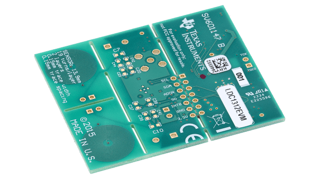
LDC1312 Evaluation Module for Inductance to Digital Converter with Sample PCB Coils
Texas Instruments
LDC1312 Evaluation Module for Inductance to Digital Converter with Sample PCB Coils
| Distributor | SKU | Stock | MOQ | 1 | 10 | 50 | 100 | 1,000 | 10,000 |
|---|---|---|---|---|---|---|---|---|---|
| DigiKey | 296-39658-ND | 1 | 1 | $118.80 | $118.80 | $118.80 | $118.80 | $118.80 | $118.80 |
| Arrow North American Components | LDC1312EVM | 0 | 1 | $114.23 | $120.45 | $120.45 | $120.45 | $120.45 | $120.45 |
| AVNET Europe | LDC1312EVM | 3 | 1 | * $48.68 | * $47.22 | * $45.27 | * $43.81 | * $43.81 | * $43.81 |
| AVNET Express | LDC1312EVM | 0 | 1 | $120.78 | $120.78 | $120.78 | $120.78 | $120.78 | $120.78 |
| element14 APAC | LDC1312EVM | 1 | 1 | * $126.16 | * $126.16 | * $126.16 | * $126.16 | * $126.16 | * $126.16 |
| Farnell | LDC1312EVM | 1 | 1 | * $117.74 | * $117.74 | * $117.74 | * $117.74 | * $117.74 | * $117.74 |
| Mouser Electronics | 595-LDC1312EVM | 5 | 1 | $131.02 | $131.02 | $131.02 | $131.02 | $131.02 | $131.02 |
| Newark | LDC1312EVM | 1 | 1 | $130.91 | $127.84 | $127.84 | $127.84 | $127.84 | $127.84 |
| RS Components | LDC1312EVM | 0 | $35.27 | ||||||
| Texas Instruments | LDC1312EVM | 18 | 1 | $99.00 | $99.00 | $99.00 | $99.00 | $99.00 | $99.00 |
| Verical Marketplace | LDC1312EVM | 1 | 1 | $141.43 | $141.43 | $141.43 | $141.43 | $141.43 | $141.43 |

EVAL-AD5172SDZ
Analog Devices Inc.
Permanent factory PCB setting Transducer adjustment of pressure, temperature, position,
| Distributor | SKU | Stock | MOQ | 1 | 10 | 50 | 100 | 1,000 | 10,000 |
|---|---|---|---|---|---|---|---|---|---|
| DigiKey | EVAL-AD5172SDZ-ND | 1 | 1 | $56.98 | $56.98 | $56.98 | $56.98 | $56.98 | $56.98 |
| Analog Devices Inc | EVAL-AD5172SDZ | 0 | $67.06 | $67.06 | $67.06 | $67.06 | $67.06 | $67.06 | |
| Arrow North American Components | EVAL-AD5172SDZ | 0 | 1 | $53.00 | $56.68 | $56.68 | $55.06 | $54.28 | $0.00 |
| element14 APAC | EVAL-AD5172SDZ | 0 | 1 | * $90.72 | * $90.72 | * $90.72 | * $90.72 | * $90.72 | * $90.72 |
| Farnell | EVAL-AD5172SDZ | 0 | 1 | * $57.13 | * $57.13 | * $57.13 | * $57.13 | * $57.13 | * $57.13 |
| Mouser Electronics | 584-EVAL-AD5172SDZ | 1 | 1 | $76.36 | $76.36 | $76.36 | $76.36 | $76.36 | $76.36 |
| Newark | EVAL-AD5172SDZ | 0 | $56.98 | $56.98 | $56.98 | $56.98 | $56.98 | $56.98 | |
| Verical Marketplace | EVAL-AD5172SDZ | 14 | 1 | $67.03 | $63.31 | $63.31 | $63.31 | $63.31 | $63.31 |

ADRV9002NP/W1/PCBZ
Analog Devices Inc.
The ADRV9002 is a highly integrated RF transceiver that has dual-channel transmitters, dual-channel receivers, integrated synthesizers, and digital signal processing functions.The ADRV9002 is a high performance, highly linear, high dynamic range transceiver designed for performance vs. power consumption system optimization. The device is configurable and ideally suited to demanding, low power, portable and battery powered equipment. The ADRV9002 operates from 30 MHz to 6000 MHz and covers the UHF, VHF, industrial, scientific, and medical (ISM) bands, and cellular frequency bands in narrow-band (kHz) and wideband operation up to 40 MHz. The ADRV9002 is capable of both TDD and FDD operation.The transceiver consists of direct conversion signal paths with state-of-the-art noise figure and linearity. Each complete receiver and transmitter subsystem includes dc offset correction, quadrature error correction (QEC), and programmable digital filters, which eliminate the need for these functions in the digital baseband. In addition, several auxiliary functions, such as auxiliary analog-to-digital converters (ADCs), auxiliary digital-to-analog converters (DACs), and general-purpose inputs/outputs (GPIOs), are integrated to provide additional monitoring and control capability.The fully integrated phase-locked loops (PLLs) provide high performance, low power, fractional-N frequency synthesis for the transmitter, receiver, and clock sections. Careful design and layout techniques provide the isolation required in high performance personal radio applications. All voltage controlled oscillator (VCO) and loop filter components are integrated to minimize the external component count. The local oscillators (LOs) have flexible configuration options and include fast lock modes.The transceiver includes low power sleep and monitor modes to save power and extend the battery life of portable devices while monitoring communications.The fully integrated, low power digital predistortion (DPD) is optimized for both narrow-band and wideband signals and enables linearization of high efficiency power amplifiers.The ADRV9002 core can be powered directly from 1.0 V, 1.3 V, and 1.8 V regulators and is controlled via a standard 4-wire serial port. Other voltage supplies are used to provide proper digital interface levels and to optimize the receiver, transmitter, and auxiliary converter performance.High data rate and low data rate interfaces are supported using configurable CMOS or low voltage differential signaling (LVDS) serial synchronous interface (SSI) choice.The ADRV9002 is packaged in a 12 mm ? 12 mm, 196-ball chip scale package ball grid array (CSP_BGA).APPLICATIONS Mission critical communications Very high frequency (VHF), ultrahigh frequency (UHF), and cellular to 6 GHz Time division duplexing (TDD) and frequency division duplexing (FDD) applications
| Distributor | SKU | Stock | MOQ | 1 | 10 | 50 | 100 | 1,000 | 10,000 |
|---|---|---|---|---|---|---|---|---|---|
| Analog Devices Inc | ADRV9002NP/W1/PCBZ | 0 | $1,843.19 | $1,843.19 | $1,843.19 | $1,843.19 | $1,843.19 | $1,843.19 | |
| element14 APAC | ADRV9002NP/W1/PCBZ | 2 | 1 | * $2,007.64 | * $2,007.64 | * $2,007.64 | * $2,007.64 | * $2,007.64 | * $2,007.64 |
| Farnell | ADRV9002NP/W1/PCBZ | 4 | 1 | * $1,938.72 | * $1,938.72 | * $1,938.72 | * $1,938.72 | * $1,938.72 | * $1,938.72 |
| Mouser Electronics | 584-ADRV9002NPW1PCBZ | 5 | 1 | $1,987.00 | $1,987.00 | $1,987.00 | $1,987.00 | $1,987.00 | $1,987.00 |
| Newark | ADRV9002NP/W1/PCBZ | 2 | 1 | $1,974.81 | $1,974.81 | $1,974.81 | $1,974.81 | $1,974.81 | $1,974.81 |

ADRV9008-1W/PCBZ
Analog Devices Inc.
The receive path consists of two independent, wide bandwidth (BW), direct conversion receivers with state-of-the-art dynamic range. The complete receive subsystem includes automatic and manual attenuation control, dc offset correction, quadrature error correction (QEC), and digital filtering, eliminating the need for these functions in the digital baseband. RF front-end control and several auxiliary functions such as analog-to-digital converters (ADCs), digital-to-analog converters (DACs), and general-purpose input/outputs (GPIOs) for the power amplifier (PA) are also integrated.In addition to automatic gain control (AGC), the ADRV9008-1 also features flexible external gain control modes, allowing significant flexibility in setting system level gain dynamically.The received signals are digitized with a set of four high dynamic range, continuous time, sigma-delta (?-?) ADCs that provide inherent antialiasing. The combination of the direct conversion architecture, which does not suffer from out of band image mixing, and the lack of aliasing relaxes the requirements of the RF filters compared to traditional intermediate frequency (IF) receivers.The fully integrated phase-locked loop (PLL) provides high per-formance, low power, fractional-N, RF synthesis for the receiver signal paths. An additional synthesizer generates the clocks needed for the converters, digital circuits, and the serial interface. A multi-chip synchronization mechanism synchronizes the phase of the RF local oscillator (LO) and baseband clocks between multiple ADRV9008-1 chips. Precautions are taken to provide the isolation required in high performance base station applications. All voltage controlled oscillators (VCOs) and loop filter components are integrated.The high speed JESD204B interface supports up to 12.288 Gbps lane rates, resulting in two lanes per transmitter and a single lane per receiver in the widest bandwidth mode. The interface also supports interleaved mode for lower bandwidths, reducing the total number of high speed data interface lanes to one. Both fixed and floating point data formats are supported. The floating point format allows internal AGC to be invisible to the demodulator device.The core of the ADRV9008-1 can be powered directly from 1.3 V and 1.8 V regulators and is controlled via a standard 4-wire serial port. Comprehensive power-down modes are included to mini-mize power consumption during normal use. The ADRV9008-1 is packaged in a 12 mm ? 12 mm, 196-ball chip scale ball grid array (CSP_BGA).Applications 3G, 4G, and 5G FDD, macrocell base stations Wide band active antenna systems Massive multiple input, multiple output (MIMO) Phased array radar Electronic warfare Military communications Portable test equipment
| Distributor | SKU | Stock | MOQ | 1 | 10 | 50 | 100 | 1,000 | 10,000 |
|---|---|---|---|---|---|---|---|---|---|
| Analog Devices Inc | ADRV9008-1W/PCBZ | 0 | $1,317.38 | $1,317.38 | $1,317.38 | $1,317.38 | $1,317.38 | $1,317.38 | |
| element14 APAC | ADRV9008-1W/PCBZ | 1 | 1 | * $1,573.58 | * $1,573.58 | * $1,573.58 | * $1,573.58 | * $1,573.58 | * $1,573.58 |
| Farnell | ADRV9008-1W/PCBZ | 1 | 1 | * $1,461.57 | * $1,461.57 | * $1,461.57 | * $1,461.57 | * $1,461.57 | * $1,461.57 |
| Mouser Electronics | 584-ADRV9008-1W/PCBZ | 2 | 1 | $1,420.17 | $1,420.17 | $1,420.17 | $1,420.17 | $1,420.17 | $1,420.17 |
| Newark | ADRV9008-1W/PCBZ | 1 | 1 | $1,371.10 | $1,371.10 | $1,371.10 | $1,371.10 | $1,371.10 | $1,371.10 |

ADRV9026-LB/PCBZ
Analog Devices Inc.
The ADRV9026 is a highly integrated, radio frequency (RF) agile transceiver offering four independently controlled transmitters, dedicated observation receiver inputs for monitoring each transmitter channel, four independently controlled receivers, integrated synthesizers, and digital signal processing functions providing a complete transceiver solution. The device provides the performance demanded by cellular infrastructure applications, such as small cell base station radios, macro 3G/4G/5G systems, and massive multiple in/multiple out (MIMO) base stations. The receiver subsystem consists of four independent, wide bandwidth, direct conversion receivers with wide dynamic range. The four independent transmitters use a direct conversion modulator resulting in low noise operation with low power consumption. The device also includes two wide bandwidth, time shared, observation path receivers with two inputs each for monitoring transmitter outputs. The complete transceiver subsystem includes automatic and manual attenuation control, dc offset correction, quadrature error correction (QEC), and digital filtering, eliminating the need for these functions in the digital baseband. Other auxiliary functions such as analog-to-digital converters (ADCs), digital-to-analog converters (DACs), and general-purpose input/outputs (GPIOs) that provide an array of digital control options are also integrated. To achieve a high level of RF performance, the transceiver includes five fully integrated phase-locked loops (PLLs). Two PLLs provide low noise and low power fractional-N RF synthesis for the transmitter and receiver signal paths. A third fully integrated PLL supports an independent local oscillator (LO) mode for the observation receiver. The fourth PLL generates the clocks needed for the converters and digital circuits, and a fifth PLL provides the clock for the serial data interface. A multichip synchronization mechanism synchronizes the phase of all LOs and baseband clocks between multiple ADRV9026 chips. All voltage controlled oscillators (VCOs) and loop filter components are integrated and adjustable through the digital control interface. The serial data interface consists of four serializer lanes and four deserializer lanes. The interface supports both the JESD204B and JESD204C standards, operating at data rates up to 24.33 Gbps. The interface also supports interleaved mode for lower bandwidths, thus reducing the number of high speed data interface lanes to one. Both fixed and floating-point data formats are supported. The floating-point format allows internal automatic gain control (AGC) to be invisible to the demodulator device. The ADRV9026 is powered directly from 1.0 V, 1.3 V, and 1.8 V regulators and is controlled via a standard serial peripheral interface (SPI) serial port. Comprehensive power-down modes are included to minimize power consumption in normal use. The ADRV9026 is packaged in a 14 mm ? 14 mm, 289-ball chip scale ball grid array (CSP_BGA).Applications 3G/4G/5G TDD and FDD massive MIMO, macro and small cell base stations
| Distributor | SKU | Stock | MOQ | 1 | 10 | 50 | 100 | 1,000 | 10,000 |
|---|---|---|---|---|---|---|---|---|---|
| Mouser Electronics | N/A | 0 |

DC1054A with DC1054B | LTC4242 Dual PCI Express Hot Swap Controller
Analog Devices Inc.
DC1054A/B: Demo Board for the LTC4242 Dual Slot Hot Swap Controller for PCI Express.
| Distributor | SKU | Stock | MOQ | 1 | 10 | 50 | 100 | 1,000 | 10,000 |
|---|---|---|---|---|---|---|---|---|---|
| Analog Devices Inc | DC1054A/B | 0 | $80.25 | $80.25 | $80.25 | $80.25 | $80.25 | $80.25 | |
| Mouser Electronics | 584-DC1054A/B | 1 | 1 | $83.05 | $83.05 | $83.05 | $83.05 | $83.05 | $83.05 |

ADCLK907/PCBZ
Analog Devices Inc.
The ADCLK905 (one input, one output), ADCLK907 (dual oneinput, one output), and ADCLK925 (one input, two outputs) areultrafast clock/data buffers fabricated on the Analog Devices, Inc.,proprietary XFCB3 silicon germanium (SiGe) bipolar process.The ADCLK905/ADCLK907/ADCLK925 feature full-swing emitter coupled logic (ECL) output drivers. For PECL (positive ECL) operation, bias VCC to the positive supply and VEE to ground. For NECL (negative ECL) operation, bias VCC to ground and VEE to the negative supply.The buffers offer 95 ps propagation delay, 7.5 GHz toggle rate, 10 Gbps data rate, and 60 fs random jitter (RJ).The inputs have center tapped, 100 ?, on-chip termination resistors. A VREF pin is available for biasing ac-coupled inputs.The ECL output stages are designed to directly drive 800 mV each side into 50 ? terminated to VCC ? 2 V for a total differential output swing of 1.6 V.The ADCLK905/ADCLK907/ADCLK925 are available in 16-lead LFCSP packages.Applications Clock and data signal restoration and level shifting Automated test equipment (ATE) High speed instrumentation High speed line receivers Threshold detection Converter clocking
| Distributor | SKU | Stock | MOQ | 1 | 10 | 50 | 100 | 1,000 | 10,000 |
|---|---|---|---|---|---|---|---|---|---|
| DigiKey | ADCLK907/PCBZ-ND | 1 | 1 | $237.62 | $237.62 | $237.62 | $237.62 | $237.62 | $237.62 |
| Analog Devices Inc | ADCLK907/PCBZ | 0 | $254.26 | $254.26 | $254.26 | $254.26 | $254.26 | $254.26 | |
| Arrow North American Components | ADCLK907/PCBZ | 0 | 1 | $221.04 | $221.04 | $221.04 | $221.04 | $221.04 | $221.04 |
| element14 APAC | ADCLK907/PCBZ | 0 | 1 | * $242.33 | * $242.33 | * $242.33 | * $242.33 | * $242.33 | * $242.33 |
| Farnell | ADCLK907/PCBZ | 0 | 1 | * $201.33 | * $201.33 | * $201.33 | * $201.33 | * $201.33 | * $201.33 |
| Mouser Electronics | 584-ADCLK907PCBZ | 3 | 1 | $263.13 | $263.13 | $263.13 | $263.13 | $263.13 | $263.13 |
| Verical Marketplace | ADCLK907/PCBZ | 45 | 1 | $271.57 | $0.00 | $0.00 | $0.00 | $0.00 | $0.00 |

ADCLK954/PCBZ
Analog Devices Inc.
The ADCLK954 is an ultrafast clock fanout buffer fabricated on the Analog Devices, Inc., proprietary XFCB3 silicon germanium (SiGe) bipolar process. This device is designed for high speed applications requiring low jitter.The device has two selectable differential inputs via the IN_SEL control pin. Both inputs are equipped with center tapped, differential, 100 ? on-chip termination resistors. The inputs accept dc-coupled LVPECL, CML, 3.3 V CMOS (single-ended), and ac-coupled 1.8 V CMOS, LVDS, and LVPECL inputs. A VREFx pin is available for biasing ac-coupled inputs.The ADCLK954 features 12 full-swing emitter coupled logic (ECL) output drivers. For LVPECL (positive ECL) operation, bias Vcc to the positive supply and VEE to ground. For ECL operation, bias VCC to ground and VEE to the negative supply.The output stages are designed to directly drive 800 mV each side into 50 ? terminated to VCC ? 2 V for a total differential output swing of 1.6 V.The ADCLK954 is available in a 40-lead LFCSP and specified for operation over the standard industrial temperature range of ?40?C to +85?C.APPLICATIONS Low jitter clock distribution Clock and data signal restoration Level translation Wireless communications Wired communications Medical and industrial imaging ATE and high performance instrumentation
| Distributor | SKU | Stock | MOQ | 1 | 10 | 50 | 100 | 1,000 | 10,000 |
|---|---|---|---|---|---|---|---|---|---|
| Analog Devices Inc | ADCLK954/PCBZ | 0 | $254.26 | $254.26 | $254.26 | $254.26 | $254.26 | $254.26 | |
| element14 APAC | ADCLK954/PCBZ | 0 | 1 | * $242.33 | * $242.33 | * $242.33 | * $242.33 | * $242.33 | * $242.33 |
| Farnell | ADCLK954/PCBZ | 0 | 1 | * $201.33 | * $201.33 | * $201.33 | * $201.33 | * $201.33 | * $201.33 |
| Mouser Electronics | 584-ADCLK954PCBZ | 3 | 1 | $263.13 | $263.13 | $263.13 | $263.13 | $263.13 | $263.13 |
| Newark | ADCLK954/PCBZ | 3 | $206.63 | $206.63 | $206.63 | $206.63 | $206.63 | $206.63 |

ADIS16265/PCBZ
Analog Devices Inc.
The ADIS16260?and ADIS16265 are programmable digital gyroscopes that combine industry-leading MEMS and signal processing technology in a single compact package. They provide accuracy performance that would require full motion calibration with any other MEMS gyroscope in their class. When power is applied, the ADIS16260 and ADIS16265 automatically start up and begin sampling sensor data, without requiring configuration commands from a system processor. An addressable register structure and a common serial peripheral interface (SPI) provide simple access to sensor data and configuration settings. Many digital processor platforms support the SPI with simple firmware-level instructions.The ADIS16260 and ADIS16265 provide several programmable features for in-system optimization. The sensor bandwidth switch (50 Hz and 330 Hz), Bartlett window FIR filter length, and sample rate settings provide users with controls that enable noise vs. bandwidth optimization. The digital input/output lines offer options for a data ready signal that helps the master processor efficiently manage data coherency, an alarm indicator signal for triggering master processor interrupts, and a general-purpose function for setting and monitoring system-level digital controls/ conditions.The ADIS16260 and ADIS16265 are drop-in replacements for the ADIS1625x family and come in LGA packages (11.2 mm ? 11.2 mm ? 5.5 mm) that meet Pb-free solder reflow profile requirements, per JEDEC J-STD-020. They have an extended operating temperature range of ?40?C to +105?C.APPLICATIONS Platform control and stabilization Navigation Medical instrumentation Robotics
| Distributor | SKU | Stock | MOQ | 1 | 10 | 50 | 100 | 1,000 | 10,000 |
|---|---|---|---|---|---|---|---|---|---|
| DigiKey | ADIS16265/PCBZ-ND | 7 | 1 | $152.48 | $152.48 | $152.48 | $152.48 | $152.48 | $152.48 |
| Analog Devices Inc | ADIS16265/PCBZ | 0 | $163.15 | $163.15 | $163.15 | $163.15 | $163.15 | $163.15 | |
| Arrow North American Components | ADIS16265/PCBZ | 0 | 1 | $132.59 | $132.59 | $132.59 | $132.59 | $132.59 | $132.59 |
| element14 APAC | ADIS16265/PCBZ | 0 | 1 | * $123.55 | * $123.55 | * $123.55 | * $123.55 | * $123.55 | * $123.55 |
| Farnell | ADIS16265/PCBZ | 1 | 1 | * $105.40 | * $105.40 | * $105.40 | * $105.40 | * $105.40 | * $105.40 |
| Mouser Electronics | 584-ADIS16265PCBZ | 1 | 1 | $168.84 | $168.84 | $168.84 | $168.84 | $168.84 | $168.84 |
| Newark | ADIS16265/PCBZ | 0 | $43.07 | $43.07 | $43.07 | $43.07 | $43.07 | $43.07 | |
| Verical Marketplace | ADIS16265/PCBZ | 22 | 1 | $165.65 | $165.65 | $165.65 | $165.65 | $165.65 | $165.65 |
| Win Source | ADIS16265/PCBZ | 6860 |