
BVX-ARM
Metcal
ARM ESD SAFE 600MM; Accessory Type:Flexible Arm; For Use With:OK International BVX-200 Series
| Distributor | SKU | Stock | MOQ | 1 | 10 | 50 | 100 | 1,000 | 10,000 |
|---|---|---|---|---|---|---|---|---|---|
| DigiKey | BVX-ARM | 11 | 1 | $129.21 | $83.00 | $104.40 | $104.40 | $104.40 | $104.40 |
| element14 APAC | BVX-ARM | 64 | 1 | * $84.04 | * $84.04 | * $84.04 | * $84.04 | * $84.04 | * $84.04 |
| Farnell | BVX-ARM | 63 | 1 | * $64.11 | * $64.11 | * $64.11 | * $64.11 | * $64.11 | * $64.11 |
| Mouser Electronics | BVX-ARM | 10 | 1 | $81.70 | $81.70 | $81.70 | $81.70 | $81.70 | $81.70 |
| Newark | BVX-ARM | 41 | 1 | $61.29 | $61.29 | $61.29 | $61.29 | $61.29 | $61.29 |
| RS Components | BVX-ARM | 0 | $56.12 | ||||||
| RS Components (APAC) | BVX-ARM | 0 | $112.18 |

| Distributor | SKU | Stock | MOQ | 1 | 10 | 50 | 100 | 1,000 | 10,000 |
|---|---|---|---|---|---|---|---|---|---|
| DigiKey | MDK-ARM-CM-FL-LC-ND | 0 | 3 | $1,535.01 | $4,610.02 | $4,610.02 | $4,610.02 | $4,610.02 | $4,610.02 |
| AVNET Express | MDK-ARM-CM | 0 | 1 | $3,840.00 | $3,840.00 | $3,840.00 | $3,840.00 | $3,840.00 | $3,840.00 |
| element14 APAC | MDK-ARM-CM | 0 | * $4,967.42 | * $4,967.42 | * $4,967.42 | * $4,967.42 | * $4,967.42 | * $4,967.42 | |
| Farnell | MDK-ARM-CM | 0 | * $3,815.62 | * $3,815.62 | * $3,815.62 | * $3,815.62 | * $3,815.62 | * $3,815.62 | |
| Mouser Electronics | N/A | 0 | 1 | $0.00 | |||||
| Newark | MDK-ARM-CM | 1 | $3,645.57 | $3,645.57 | $3,645.57 | $3,645.57 | $3,645.57 | $3,645.57 |

| Distributor | SKU | Stock | MOQ | 1 | 10 | 50 | 100 | 1,000 | 10,000 |
|---|---|---|---|---|---|---|---|---|---|
| DigiKey | 685-MDK000MDKESSENTIALKEIL-NLPERP-ND | 0 | $3,840.02 | $3,840.02 | $3,840.02 | $3,840.02 | $3,840.02 | $3,840.02 | |
| AVNET Express | MDK-ARM-CM-LC | 0 | 1 | $0.00 | $0.00 | $0.00 | $0.00 | $0.00 | $0.00 |
| element14 APAC | MDK-ARM-CM-LC | 100 | * $4,967.42 | * $4,967.42 | * $4,967.42 | * $4,967.42 | * $4,967.42 | * $4,967.42 | |
| Farnell | MDK-ARM-CM-LC | 100 | * $3,815.62 | * $3,815.62 | * $3,815.62 | * $3,815.62 | * $3,815.62 | * $3,815.62 | |
| Mouser Electronics | N/A | 0 | 1 |
1AHC-DESK-ARM-REST
StarTech.com
Adjustable Arm Rest, Office Desk, Blk Rohs Compliant: Yes |Startech 1AHC-DESK-ARM-REST
| Distributor | SKU | Stock | MOQ | 1 | 10 | 50 | 100 | 1,000 | 10,000 |
|---|---|---|---|---|---|---|---|---|---|
| DigiKey | 1AHC-DESK-ARM-REST | 0 | 1 | $40.52 | $40.52 | $40.52 | $40.52 | $40.52 | $40.52 |
| Farnell | 1AHC-DESK-ARM-REST | 7 | 1 | * $38.45 | * $38.45 | * $38.45 | * $38.45 | * $38.45 | * $38.45 |
| Newark | 1AHC-DESK-ARM-REST | 12 | 1 | $38.63 | $38.63 | $38.63 | $38.63 | $38.63 | $38.63 |
| Distributor | SKU | Stock | MOQ | 1 | 10 | 50 | 100 | 1,000 | 10,000 |
|---|---|---|---|---|---|---|---|---|---|
| AVNET Europe | EWARM-CM-FSL | 0 | 1 | * $0.00 | * $0.00 | * $0.00 | * $0.00 | * $0.00 | * $0.00 |
| Mouser Electronics | 841-EWARM-CM-FSL | 0 | 1 |
| Distributor | SKU | Stock | MOQ | 1 | 10 | 50 | 100 | 1,000 | 10,000 |
|---|---|---|---|---|---|---|---|---|---|
| AVNET Europe | DEMORADARMCU7TOBO1 | 0 | 1 | * $801.02 | * $742.97 | * $568.84 | * $515.44 | * $515.44 | * $515.44 |
| Mouser Electronics | 726-DEMORADARMCU7TOB | 1 | 1 | $286.02 | $286.02 | $286.02 | $286.02 | $286.02 | $286.02 |

ADP1883ARMZ-0.6-R7
Analog Devices Inc.
The ADP1882 / ADP1883 are versatile current-mode, synchronous step-down controllers that provide superior transient response, optimal stability, and current-limit protection by using a constant on-time, pseudo-fixed frequency with a programmable current-limit, current-control scheme. In addition, these devices offer optimum performance at low duty cycles by using valley current-mode control architecture. This allows the ADP1882 / ADP1883 to drive all N-channel power stages to regulate output voltages as low as 0.8 V.The ADP1883 is the power saving mode (PSM) version of the device and is capable of pulse skipping to maintain output regulation while achieving improved system efficiency at light loads (see the Power Saving Mode (PSM) Version (ADP1883) section for more information).Available in three frequency options (300 kHz, 600 kHz, and 1.0 MHz, plus the PSM option), the ADP1882/ADP1883 are well suited for a wide range of applications. These ICs not only operate from a 2.75 V to 5.5 V bias supply, but they also can accept a power input as high as 20 V.In addition, an internally fixed soft start period is included to limit input in-rush current from the input supply during startup and to provide reverse current protection during soft start for a pre-charged output. The low-side current-sense, current-gain scheme and integration of a boost diode, along with the PSM/forced pulse-width modulation (PWM) option, reduce the external part count and improve efficiency.The ADP1882 / ADP1883 operate over the -40°C to +125°C junction temperature range and are available in a 10-lead MSOP.
| Distributor | SKU | Stock | MOQ | 1 | 10 | 50 | 100 | 1,000 | 10,000 |
|---|---|---|---|---|---|---|---|---|---|
| DigiKey | ADP1883ARMZ-0.6-R7 | 1000 | 1 | $3.24 | $2.43 | $2.23 | $2.00 | $1.78 | $1.69 |
| Analog Devices Inc | ADP1883ARMZ-0.6-R7 | 0 | $3.26 | $2.93 | $2.77 | $2.40 | $1.74 | $1.74 | |
| Arrow North American Components | ADP1883ARMZ-0.6-R7 | 0 | 1000 | $1.39 | $1.39 | ||||
| Farnell | ADP1883ARMZ-0.6-R7 | 0 | 10 | $2.00 | $1.59 | $1.11 | $0.88 | $0.88 | $0.88 |
| Verical Marketplace | ADP1883ARMZ-0.6-R7 | 5000 | 1000 | $1.43 | $1.43 |

| Distributor | SKU | Stock | MOQ | 1 | 10 | 50 | 100 | 1,000 | 10,000 |
|---|---|---|---|---|---|---|---|---|---|
| DigiKey | ADR3630ARMZ | 0 | 1000 | $8.63 | $6.70 | $5.93 | $5.69 | $5.16 | $5.16 |
| Arrow North American Components | ADR3630ARMZ | 35 | 1 | $1.56 | $1.55 | $1.54 | $1.54 | $0.00 | $0.00 |
| element14 APAC | ADR3630ARMZ | 31 | 1 | * $9.62 | * $7.47 | * $6.62 | * $6.35 | * $6.06 | * $6.06 |
| Farnell | ADR3630ARMZ | 31 | 1 | * $9.99 | * $8.53 | * $7.24 | * $6.69 | * $6.44 | * $6.44 |
| Newark | ADR3630ARMZ | 33 | 1 | $8.89 | $6.90 | $6.11 | $5.86 | $5.86 | $5.86 |
| Verical Marketplace | ADR3630ARMZ | 1500 | 100 | $4.03 | $4.03 | $4.03 |
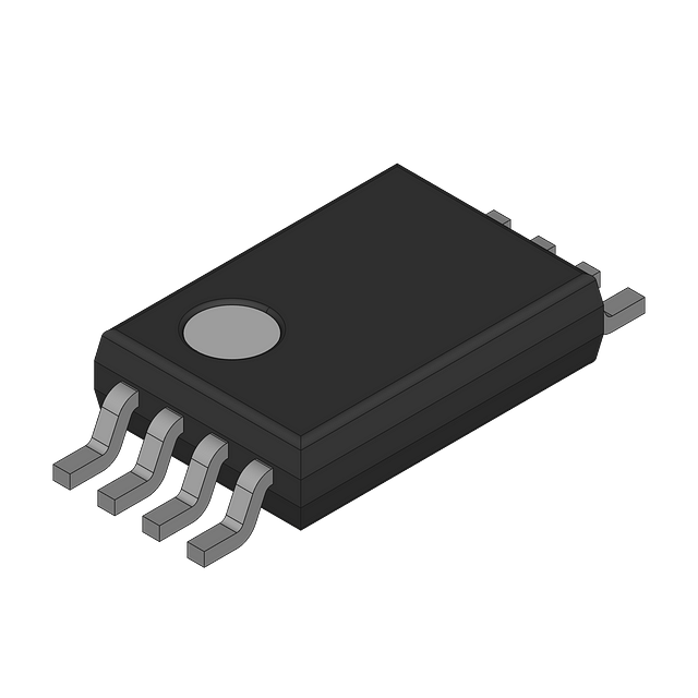
AD7683ARM
Analog Devices Inc.
ADC, Successive Approximation, 16-Bit, 1 Func, 1 Channel, Serial Access, CMOS, PDSO8
| Distributor | SKU | Stock | MOQ | 1 | 10 | 50 | 100 | 1,000 | 10,000 |
|---|---|---|---|---|---|---|---|---|---|
| DigiKey | 505-AD7683ARMZ-ND | 843 | 1 | $20.56 | $16.42 | $14.77 | $14.25 | $13.12 | $13.12 |
| Win Source | AD7683ARM | 1 | 1 |