| Distributor | SKU | Stock | MOQ | 1 | 10 | 50 | 100 | 1,000 | 10,000 |
|---|---|---|---|---|---|---|---|---|---|
| DigiKey | A165L-ARM-5D-2 | 10 | 1 | $45.25 | $41.18 | $36.63 | $35.19 | $28.73 | $28.73 |
| AVNET Express | A165L-ARM-5D-2 | 0 | 1 | $44.91 | $42.28 | $38.13 | $38.13 | $38.13 | $38.13 |
| Mouser Electronics | A165L-ARM-5D-2 | 3 | 1 | $48.25 | $40.54 | $34.75 | $32.58 | $32.37 | $32.37 |
| Newark | A165L-ARM-5D-2 | 0 | 1 | $75.75 | $66.01 | $58.10 | $58.10 | $58.10 | $58.10 |
| Distributor | SKU | Stock | MOQ | 1 | 10 | 50 | 100 | 1,000 | 10,000 |
|---|---|---|---|---|---|---|---|---|---|
| DigiKey | A165L-ARM-24-1 | 0 | $20.11 | $20.11 | $20.11 | $20.11 | $20.11 | $20.11 | |
| AVNET Express | A165L-ARM-24-1 | 0 | 1 | $0.00 | $0.00 | $0.00 | $0.00 | $0.00 | $0.00 |
| Mouser Electronics | A165L-ARM-24-1 | 0 | 1 | $25.44 | $24.36 | $21.50 | $20.79 | $19.19 | $19.19 |
| Distributor | SKU | Stock | MOQ | 1 | 10 | 50 | 100 | 1,000 | 10,000 |
|---|---|---|---|---|---|---|---|---|---|
| DigiKey | A16L-ARM-12D-1 | 0 | $25.67 | $25.67 | $25.67 | $25.67 | $25.67 | $25.67 | |
| AVNET Express | A16L-ARM-12D-1 | 0 | 1 | $35.70 | $31.53 | $30.95 | $30.95 | $30.95 | $30.95 |
| Mouser Electronics | A16L-ARM-12D-1 | 7 | 1 | $32.92 | $31.14 | $27.46 | $26.56 | $25.64 | $25.64 |
| Distributor | SKU | Stock | MOQ | 1 | 10 | 50 | 100 | 1,000 | 10,000 |
|---|---|---|---|---|---|---|---|---|---|
| DigiKey | CP15774_CARMEN-S-C | 0 | 1 | $7.21 | $7.21 | $5.23 | $4.48 | $3.61 | $2,010.00 |
| Ameya360 | CP15774_CARMEN-S-C | 150 | |||||||
| Arrow North American Components | CP15774_CARMEN-S-C | 0 | 150 | $0.00 | $0.00 | $0.00 | $0.00 | $2.88 | $6.20 |
| AVNET Europe | CP15774_CARMEN-S-C | 148 | 15 | * $3.11 | * $2.93 | ||||
| AVNET Express | CP15774_CARMEN-S-C | 0 | 15 | $2.67 | $2.21 | ||||
| Future Electronics | CP15774_CARMEN-S-C | 150 | 150 | $3.83 | |||||
| Mouser Electronics | CP15774_CARMEN-S-C | 15 | 1 | $7.23 | $5.24 | $4.83 | $4.83 | $3.60 | $3.51 |
| Newark | CP15774_CARMEN-S-C | 0 | 15 | $5.71 | $4.85 | $4.52 | $3.77 | $3.77 | |
| RS Components | CP15774_CARMEN-S-C | 0 | $7.75 | ||||||
| RS Components (APAC) | CP15774_CARMEN-S-C | 0 | $12.45 |
| Distributor | SKU | Stock | MOQ | 1 | 10 | 50 | 100 | 1,000 | 10,000 |
|---|---|---|---|---|---|---|---|---|---|
| DigiKey | ADT7421ARMZ-RL7 | 0 | 349 | $0.00 | $0.00 | ||||
| AVNET Express | ADT7421ARMZ-RL7 | 548 | 1000 | $0.00 | $0.00 | ||||
| Mouser Electronics | ADT7421ARMZ-RL7 | 0 | 1 | ||||||
| Win Source | ADT7421ARMZ-RL7 | 3123 | 120 |
| Distributor | SKU | Stock | MOQ | 1 | 10 | 50 | 100 | 1,000 | 10,000 |
|---|---|---|---|---|---|---|---|---|---|
| DigiKey | ADT7488AARMZ-REEL7CT-ND | 0 | $0.00 | $0.00 | $0.00 | $0.00 | $0.00 | $0.00 | |
| Mouser Electronics | N/A | 0 | |||||||
| Win Source | ADT7488AARMZ-REEL7 | 2750 | 5 |
| Distributor | SKU | Stock | MOQ | 1 | 10 | 50 | 100 | 1,000 | 10,000 |
|---|---|---|---|---|---|---|---|---|---|
| DigiKey | ADT7461AARMZ-002 | 0 | $0.00 | $0.00 | |||||
| AVNET Express | ADT7461AARMZ-002 | 0 | 50 | $0.00 | $0.00 | ||||
| Mouser Electronics | ADT7461AARMZ-002 | 0 | 1 |
| Distributor | SKU | Stock | MOQ | 1 | 10 | 50 | 100 | 1,000 | 10,000 |
|---|---|---|---|---|---|---|---|---|---|
| DigiKey | ADT7421ARMZ-2RL7-ND | 0 | $363.00 | $6,000.00 | |||||
| AVNET Express | ADT7421ARMZ-2RL | 196706 | 1 | $0.56 | $0.51 | ||||
| Farnell | ADT7421ARMZ-2RL | 56706 | 250 | * $0.00 | * $0.00 | * $0.00 | * $0.00 | * $0.64 | * $0.64 |
| Mouser Electronics | 863-ADT7421ARMZ-2RL | 0 | 1 | ||||||
| Newark | ADT7421ARMZ-2RL | 0 | 650 | $0.00 | $0.00 | $0.00 | $0.00 | $0.65 | $0.51 |
| Perceptive | ADT7421ARMZ-2RL | 7130 | 1+ | $0.00 | $0.00 | $0.00 | $0.00 | $0.00 | $0.00 |
| Verical Marketplace | ADT7421ARMZ-2RL | 202203 | 455 | $0.69 | $0.61 | ||||
| Win Source | ADT7421ARMZ-2RL | 7900 | 5 |
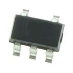
S-8520B27MC-ARMT2G
ABLIC Inc.
DC DC Cntrlr Single-OUT PWM DC to DC Controller/Step Down 2.5V to 16V Input 5-Pin SOT-23 T/R
| Distributor | SKU | Stock | MOQ | 1 | 10 | 50 | 100 | 1,000 | 10,000 |
|---|---|---|---|---|---|---|---|---|---|
| DigiKey | S-8520B27MC-ARMT2G | 0 | 3000 | $0.52 | |||||
| AVNET Express | S-8520B27MC-ARMT2G | 0 | 3000 | $0.51 | $0.51 | $0.51 | $0.51 | $0.51 | $0.51 |
| Mouser Electronics | S-8520B27MC-ARMT2G | 0 | 3000 | $0.55 |

| Distributor | SKU | Stock | MOQ | 1 | 10 | 50 | 100 | 1,000 | 10,000 |
|---|---|---|---|---|---|---|---|---|---|
| DigiKey | C16752_CARMEN-70-SHD | 0 | 150 | $1.24 | $1.24 | ||||
| AVNET Europe | C16752_CARMEN-70-SHD | 135 | 15 | * $0.93 | * $0.88 | ||||
| AVNET Express | C16752_CARMEN-70-SHD | 0 | 15 | $0.75 | $0.64 | ||||
| Mouser Electronics | C16752_CARMEN-70-SHD | 0 | 1 | $2.33 | $1.55 | $1.55 | $1.55 | $1.11 | $0.98 |
| Newark | C16752_CARMEN-70-SHD | 0 | 150 | $0.00 | $0.00 | $0.00 | $1.10 | $0.89 | $0.89 |