|
|
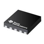
Texas Instruments
UCC27201AQDMKRQ1
|
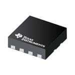
Texas Instruments
UCC27201DRMR
|
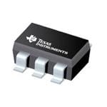
Texas Instruments
UCC27531DBVT
|

Texas Instruments
UCC27538DBVR
|

Texas Instruments
UCC27538DBVT
|
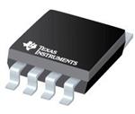
Texas Instruments
UCC28810DRG4
|

Texas Instruments
UCC28810DR
|
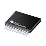
Texas Instruments
V62/05615-01XE
|
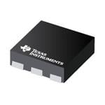
Texas Instruments
VSP1000DSFR
|
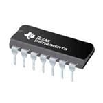
Texas Instruments
XTR105PAG4
|
| Price |
|
|
|
|
|
|
|
|
|
|
|
| RoHS |
|
Compliant |
Compliant |
Compliant |
Compliant |
Compliant |
Compliant |
Compliant |
Compliant |
Compliant |
Compliant |
| Lead Status |
|
No |
No |
No |
No |
No |
No |
No |
No |
No |
No |
| Rise Time(ns) |
|
8 |
8 |
15 |
15 |
15 |
|
|
|
|
|
| Input VCC(Max)(V) |
|
17 |
17 |
32 |
32 |
32 |
|
|
|
|
|
| Power Switch |
|
MOSFET |
MOSFET |
MOSFET,IGBT,SiCFET |
MOSFET,IGBT,SiCFET |
MOSFET,IGBT,SiCFET |
|
|
|
|
|
| Operating Temperature Range(C) |
|
-40 to 125 |
-40 to 140 |
-40 to 125,-40 to 140 |
-40 to 140 |
-40 to 140 |
-40 to 105 |
-40 to 105 |
-40 to 125 |
0 to 85 |
|
| Rating |
|
Automotive |
Catalog |
Catalog |
Catalog |
Catalog |
Catalog |
Catalog |
HiRel Enhanced Product |
Catalog |
|
| Iq(uA) |
|
1 |
1 |
250 |
250 |
250 |
|
|
|
|
|
| Input VCC(Min)(V) |
|
8 |
8 |
10 |
10 |
10 |
|
|
|
|
|
| Number of Channels(#) |
|
2 |
2 |
1 |
1 |
1 |
|
|
|
1 |
|
| Fall Time(ns) |
|
7 |
7 |
7 |
7 |
7 |
|
|
|
|
|
| Negative Voltage Handling at HS Pin(V) |
|
-15 |
-1 |
|
|
|
|
|
|
|
|
| Channel Input Logic |
|
TTL |
TTL |
Non-Inverting,Single |
Dual,Non-Inverting |
Dual,Non-Inverting |
|
|
|
|
|
| Prop Delay(ns) |
|
20 |
20 |
17 |
17 |
17 |
|
|
|
|
|
| Package Group |
|
SO PowerPAD,VSON |
SO PowerPAD,SOIC,VSON |
SOIC,SOT-23 |
SOT-23 |
SOT-23 |
SOIC |
SOIC |
TSSOP |
SON |
PDIP,SOIC |
| Approx. Price (US$) |
|
1.53 | 1ku |
1.30 | 1ku |
0.75 | 1ku |
0.75 | 1ku |
0.75 | 1ku |
0.25 | 1ku |
0.25 | 1ku |
|
0.37 | 1ku |
4.60 | 1ku |
| Peak Output Current(A) |
|
3 |
3 |
5 |
5 |
5 |
|
|
|
|
|
| Bus Voltage(V) |
|
110 |
110 |
|
|
|
|
|
|
|
|
| Input Threshold |
|
|
|
CMOS,TTL |
CMOS,TTL |
CMOS,TTL |
|
|
|
|
|
| Special Features |
|
|
|
Split Output |
Split Output |
Split Output |
Adjustable Switch Frequency,Soft Start,Soft Switching |
Adjustable Switch Frequency,Soft Start,Soft Switching |
|
|
|
| Input Negative Voltage(V) |
|
|
|
-5 |
-5 |
-5 |
|
|
|
|
|
| Switching Frequency(Max)(kHz) |
|
|
|
|
|
|
250 |
250 |
|
|
|
| Switching Frequency(Min)(kHz) |
|
|
|
|
|
|
5 |
5 |
|
|
|
| Type |
|
|
|
|
|
|
Inductive |
Inductive |
|
|
|
| Comments |
|
|
|
|
|
|
0 |
0 |
|
|
|
| Vout(Min)(V) |
|
|
|
|
|
|
9 |
9 |
|
|
|
| Vin(Min)(V) |
|
|
|
|
|
|
13 |
13 |
|
|
|
| Topology |
|
|
|
|
|
|
Boost,Buck,Flyback,PFC Controller,Sepic |
Boost,Buck,Flyback,PFC Controller,Sepic |
|
|
|
| Regulated Outputs(#) |
|
|
|
|
|
|
1 |
1 |
|
|
|
| Dimming Method |
|
|
|
|
|
|
Analog |
Analog |
|
|
|
| Package Size |
|
|
|
|
|
|
mm2 |
mm2 |
mm2 |
mm2 |
mm2 |
| Iout(Max)(A) |
|
|
|
|
|
|
5 |
5 |
|
|
|
| Vout(Max)(V) |
|
|
|
|
|
|
400 |
400 |
|
|
|
| Power Factor Correction(Min) |
|
|
|
|
|
|
Active |
Active |
|
|
|
| Vin(Max)(V) |
|
|
|
|
|
|
18 |
18 |
|
|
|
| Iq(Typ)(mA) |
|
|
|
|
|
|
4 |
4 |
|
|
|
| Input Voltage(Type) |
|
|
|
|
|
|
AC/DC |
AC/DC |
|
|
|
| Vref(V) |
|
|
|
|
|
|
2.5 |
2.5 |
|
|
|
| No. of Tx |
|
|
|
|
|
|
|
|
1 |
|
|
| Signaling Rate(Mbps) |
|
|
|
|
|
|
|
|
125 |
|
|
| Input Signal |
|
|
|
|
|
|
|
|
LVDS,LVTTL |
|
|
| ESD HBM(kV) |
|
|
|
|
|
|
|
|
12 |
|
|
| No. of Rx |
|
|
|
|
|
|
|
|
4 |
|
|
| Output Signal |
|
|
|
|
|
|
|
|
LVDS,LVTTL |
|
|
| ICC(Max)(mA) |
|
|
|
|
|
|
|
|
25 |
|
|
| Pd(Typ)(mW) |
|
|
|
|
|
|
|
|
|
20 |
|
| Gain(Max)(dB) |
|
|
|
|
|
|
|
|
|
1 |
|
| Gain(Min)(dB) |
|
|
|
|
|
|
|
|
|
1 |
|
| Output Data Format |
|
|
|
|
|
|
|
|
|
Analog |
|
| Supply Voltage(s)(V) |
|
|
|
|
|
|
|
|
|
14 |
|
| Vs(Max)(V) |
|
|
|
|
|
|
|
|
|
|
36 |
| Output Zero Error (+/-)(Max)(uA) |
|
|
|
|
|
|
|
|
|
|
25 |
| CMRR, 60Hz(Min)(dB) |
|
|
|
|
|
|
|
|
|
|
86 |
| Output Range(mA) |
|
|
|
|
|
|
|
|
|
|
4 to 20 |
| Offset Voltage Drift (+/-)(Max)(uV/Degrees Celsius) |
|
|
|
|
|
|
|
|
|
|
1.5 |
| Vs(Min)(V) |
|
|
|
|
|
|
|
|
|
|
7.5 |
| Auxiliary Output Voltage(V) |
|
|
|
|
|
|
|
|
|
|
5.1 |
| Span Error(Max)(%) |
|
|
|
|
|
|
|
|
|
|
0.2 |
| Sensor Excitation |
|
|
|
|
|
|
|
|
|
|
Two 800uA sources |
| Loop Voltage(V) |
|
|
|
|
|
|
|
|
|
|
7.5 to 36 |
| Non-Linearity(Max)(%) |
|
|
|
|
|
|
|
|
|
|
0.01 |
| Offset Voltage (+/-)(Max)(uV) |
|
|
|
|
|
|
|
|
|
|
25 |
| Full Scale Input Range |
|
|
|
|
|
|
|
|
|
|
5mV to 1V |