S25FL064LABNFV010
Infineon Technologies AG
NOR Flash 64Mbit 16M X 4Bit/32M X 2Bit/64M X 1Bit Serial-SPI 8-Pin SOIC Tray
| Distributor | SKU | Stock | MOQ | 1 | 10 | 50 | 100 | 1,000 | 10,000 |
|---|---|---|---|---|---|---|---|---|---|
| DigiKey | S25FL064LABNFV010 | 0 | 1 | $1.58 | $1.48 | $50.00 | $100.00 | $1.27 | $5,390.00 |
| Arrow North American Components | S25FL064LABNFV010 | 0 | 4900 | $0.77 | |||||
| AVNET Europe | S25FL064LABNFV010 | 0 | 490 | * $1.19 | * $1.00 | ||||
| AVNET Express | S25FL064LABNFV010 | 0 | 1 | $0.79 | $0.75 | ||||
| Farnell | S25FL064LABNFV010 | 0 | 1 | * $1.73 | * $1.63 | * $1.59 | * $1.51 | * $1.47 | * $1.47 |
| Mouser Electronics | S25FL064LABNFV010 | 3922 | 1 | $1.42 | $1.14 | $1.14 | $1.04 | $1.04 | $1.04 |
| Newark | S25FL064LABNFV010 | 0 | 1 | $1.63 | $1.52 | $1.52 | $1.42 | $1.31 | $1.31 |
| Verical Marketplace | S25FL064LABNFV010 | 7004 | 276 | $1.13 | $1.01 |
S25FL256SAGMFIG00
Infineon Technologies AG
NOR Flash 256Mbit 64M X 4Bit/128M X 2Bit/256M X 1Bit Serial-SPI 3V 16-Pin SOIC
| Distributor | SKU | Stock | MOQ | 1 | 10 | 50 | 100 | 1,000 | 10,000 |
|---|---|---|---|---|---|---|---|---|---|
| DigiKey | S25FL256SAGMFIG00 | 3876 | 1 | $4.96 | $4.63 | $4.39 | $4.79 | $4.29 | $3.91 |
| Arrow North American Components | S25FL256SAGMFIG00 | 0 | 2400 | $2.95 | |||||
| AVNET Asia Pacific | S25FL256SAGMFIG00 | 0 | 240 | ||||||
| AVNET Express | S25FL256SAGMFIG00 | 240 | 1 | $2.21 | $2.12 | ||||
| Farnell | S25FL256SAGMFIG00 | 0 | 1 | * $5.15 | * $4.81 | * $4.56 | * $4.22 | * $4.22 | * $4.22 |
| Mouser Electronics | S25FL256SAGMFIG00 | 2160 | 1 | $5.80 | $5.04 | $5.04 | $4.40 | $4.02 | $3.72 |
| Newark | S25FL256SAGMFIG00 | 0 | 1 | $5.35 | $4.99 | $4.73 | $4.59 | $4.59 | $4.59 |
| Verical Marketplace | S25FL256SAGMFIG00 | 7436 | 338 | $2.20 | $2.20 |
S25FL064LABMFB011
Infineon Technologies AG
NOR Flash 64Mbit 16M X 4Bit/32M X 2Bit/64M X 1Bit Serial-SPI 8-Pin SOIC Tube
| Distributor | SKU | Stock | MOQ | 1 | 10 | 50 | 100 | 1,000 | 10,000 |
|---|---|---|---|---|---|---|---|---|---|
| DigiKey | S25FL064LABMFB011 | 1472 | 1 | $1.77 | $1.66 | $1.61 | $1.54 | $1.45 | $1.34 |
| Arrow North American Components | S25FL064LABMFB011 | 0 | 2275 | $0.99 | |||||
| AVNET Express | S25FL064LABMFB011 | 0 | 2275 | $1.15 | |||||
| Farnell | S25FL064LABMFB011 | 0 | 1 | * $1.90 | * $1.78 | * $1.73 | * $1.64 | * $1.63 | * $1.63 |
| Mouser Electronics | S25FL064LABMFB011 | 5365 | 1 | $2.00 | $1.63 | $1.63 | $1.54 | $1.44 | $1.32 |
| Newark | S25FL064LABMFB011 | 0 | 1 | $1.79 | $1.69 | $1.69 | $1.55 | $1.33 | $1.33 |
S25FL256SAGNFV001
Infineon Technologies AG
NOR Flash 256Mbit 64M X 4Bit/128M X 2Bit/256M X 1Bit Serial-SPI 3V 8-Pin WSON
| Distributor | SKU | Stock | MOQ | 1 | 10 | 50 | 100 | 1,000 | 10,000 |
|---|---|---|---|---|---|---|---|---|---|
| DigiKey | S25FL256SAGNFV001 | 4837 | 1 | $5.60 | $5.22 | $5.07 | $4.86 | $574.00 | $1,066.00 |
| Arrow North American Components | S25FL256SAGNFV001 | 0 | 2050 | $3.15 | |||||
| AVNET Express | S25FL256SAGNFV001 | 668 | 2050 | $3.45 | |||||
| element14 APAC | S25FL256SAGNFV001 | 0 | 1 | * $7.26 | * $6.73 | * $6.33 | * $6.12 | * $6.12 | * $6.12 |
| Farnell | S25FL256SAGNFV001 | 0 | 1 | * $5.61 | * $5.23 | * $4.88 | * $4.76 | * $4.76 | * $4.76 |
| Mouser Electronics | S25FL256SAGNFV001 | 383 | 1 | $4.71 | $3.75 | $3.75 | $3.73 | $3.73 | $3.73 |
| Newark | S25FL256SAGNFV001 | 0 | 1 | $5.09 | $4.79 | $4.54 | $4.45 | $4.45 | $4.45 |
| Verical Marketplace | S25FL256SAGNFV001 | 1607 | 97 | $3.89 | $3.30 | $3.11 |

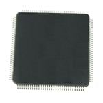
S29GL128P11TFI010
Infineon Technologies AG
S29GL128P Series 128 Mb (16M x 8) 3 V 110 ns SMT Flash-NOR Memory - TSOP-56
| Distributor | SKU | Stock | MOQ | 1 | 10 | 50 | 100 | 1,000 | 10,000 |
|---|---|---|---|---|---|---|---|---|---|
| DigiKey | S29GL128P11TFI010 | 0 | 910 | $6.97 | $6.18 | $5.75 | $5.51 | $6.18 | $6.18 |
| AVNET Express | S29GL128P11TFI010 | 903 | 91 | $0.00 | $0.00 | ||||
| Farnell | S29GL128P11TFI010 | 0 | 1 | * $4.65 | * $3.85 | * $3.18 | * $3.18 | * $3.18 | * $3.18 |
| Future Electronics | S29GL128P11TFI010 | 14 | 1 | $0.00 | $0.00 | $0.00 | $3.70 | $3.70 | $3.70 |
| Mouser Electronics | S29GL128P11TFI010 | 848 | 1 | $6.87 | $5.44 | $5.44 | $5.43 | $4.97 | $4.97 |
| Verical Marketplace | S29GL128P11TFI010 | 465 | 69 | $5.19 | $4.64 | $4.38 |
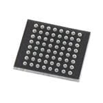
S29GL128P90FFIR20
Infineon Technologies AG
S29GL128P Series 128 Mb (16M x 8) 3 V 90 ns Flash-NOR Memory - BGA-64
| Distributor | SKU | Stock | MOQ | 1 | 10 | 50 | 100 | 1,000 | 10,000 |
|---|---|---|---|---|---|---|---|---|---|
| DigiKey | S29GL128P90FFIR20 | 0 | 180 | ||||||
| AVNET Express | S29GL128P90FFIR20 | 65 | 180 | $0.00 | |||||
| element14 APAC | S29GL128P90FFIR20 | 880 | 1 | $10.75 | |||||
| Farnell | S29GL128P90FFIR20 | 195 | 900 | $3.83 | |||||
| Future Electronics | S29GL128P90FFIR20 | 40 | 1 | $4.11 | |||||
| Mouser Electronics | S29GL128P90FFIR20 | 700 | 1 | ||||||
| Newark | S29GL128P90FFIR20 | 195 | 1 | $7.08 | |||||
| Rutronik | S29GL128P90FFIR20 | 180 | 900 | $6.15 | |||||
| TME | S29GL128P90FFIR20 | 19 | $8.16 |
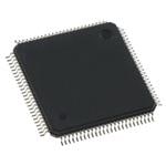
CY8C3244AXI-153
Infineon Technologies AG
MCU 8-Bit PSoC 8051 CISC 16k-Byte Flash 2.5V/3.3V/5V 100-Pin TQFP Tray
| Distributor | SKU | Stock | MOQ | 1 | 10 | 50 | 100 | 1,000 | 10,000 |
|---|---|---|---|---|---|---|---|---|---|
| DigiKey | CY8C3244AXI-153 | 0 | 1500 | $9.24 | $7.19 | $5.34 | $6.15 | $5.69 | $5.48 |
| Arrow North American Components | CY8C3244AXI-153 | 0 | 450 | $4.85 | $4.85 | ||||
| AVNET Asia Pacific | CY8C3244AXI-153 | 0 | 450 | ||||||
| AVNET Express | CY8C3244AXI-153 | 229 | 450 | $5.46 | $5.05 | ||||
| element14 APAC | CY8C3244AXI-153 | 0 | 1 | * $8.41 | * $7.50 | * $6.75 | * $6.75 | * $5.55 | * $5.55 |
| Farnell | CY8C3244AXI-153 | 0 | 1 | * $5.38 | * $4.40 | * $3.73 | * $3.29 | * $3.29 | * $3.29 |
| Mouser Electronics | CY8C3244AXI-153 | 198 | 1 | $7.39 | $5.74 | $5.25 | $5.25 | $5.25 | $5.25 |
AEK-AUD-C1D9031
STMicroelectronics
AVAS solution based on SPC582B60E1 Chorus family MCU &F DA903D Class D audio amp
| Distributor | SKU | Stock | MOQ | 1 | 10 | 50 | 100 | 1,000 | 10,000 |
|---|---|---|---|---|---|---|---|---|---|
| DigiKey | AEK-AUD-C1D9031 | 13 | 1 | $131.18 | $131.18 | $131.18 | $131.18 | $131.18 | $131.18 |
| Anglia | AEK-AUD-C1D9031 | 2 | |||||||
| Arrow North American Components | AEK-AUD-C1D9031 | 6 | 1 | $25.11 | $25.11 | $25.11 | $25.11 | $25.11 | $25.11 |
| AVNET Europe | AEK-AUD-C1D9031 | 0 | 1 | ||||||
| AVNET Express | AEK-AUD-C1D9031 | 20 | 1 | $0.00 | $0.00 | $0.00 | $0.00 | $0.00 | $0.00 |
| element14 APAC | AEK-AUD-C1D9031 | 1 | 1 | * $132.24 | * $132.24 | * $132.24 | * $132.24 | * $132.24 | * $132.24 |
| Farnell | AEK-AUD-C1D9031 | 1 | 1 | * $109.10 | * $109.10 | * $109.10 | * $109.10 | * $109.10 | * $109.10 |
| Future Electronics | AEK-AUD-C1D9031 | 8 | 1 | $135.45 | |||||
| Mouser Electronics | AEK-AUD-C1D9031 | 7 | 1 | $135.84 | $135.84 | $135.84 | $135.84 | $135.84 | $135.84 |
| Newark | AEK-AUD-C1D9031 | 1 | 1 | $163.72 | $163.72 | $163.72 | $163.72 | $163.72 | $163.72 |
| RS Components | AEK-AUD-C1D9031 | 0 | $119.96 | ||||||
| RS Components (APAC) | AEK-AUD-C1D9031 | 0 | $256.52 | ||||||
| Verical Marketplace | AEK-AUD-C1D9031 | 6 | 1 | $143.67 | $143.67 | $143.67 | $143.67 | $143.67 | $143.67 |

| Distributor | SKU | Stock | MOQ | 1 | 10 | 50 | 100 | 1,000 | 10,000 |
|---|---|---|---|---|---|---|---|---|---|
| DigiKey | AT88SC12816C-PU-ND | 124 | 1 | $1.21 | $1.21 | $1.19 | $1.06 | $1.06 | $1.06 |
| Mouser Electronics | N/A | 0 |
| Distributor | SKU | Stock | MOQ | 1 | 10 | 50 | 100 | 1,000 | 10,000 |
|---|---|---|---|---|---|---|---|---|---|
| DigiKey | DS21Q41BT-ND | 0 | $0.00 | ||||||
| AVNET Express | DS21Q41BT | 51 | 1 | $82.63 | $82.63 | $82.63 | $82.63 | $82.63 | $82.63 |
| Mouser Electronics | 700-DS21Q41BT | 0 | 1 | ||||||
| Win Source | DS21Q41BT | 11200 | 9 |