|
|
Texas Instruments
OPA348AIDR
|
Texas Instruments
PCA9534DBR
|
Texas Instruments
PCA9534PW
|
Texas Instruments
PCA9536DGKR
|
Texas Instruments
PCM1870RHFT
|
Texas Instruments
PLPV811DBVT
|
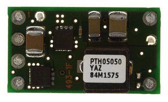
Texas Instruments
PTH03000WAS
|

Texas Instruments
PTH03020WAS
|

Texas Instruments
PTH03050WAST
|

Texas Instruments
PTH03060WAD
|
| Price |
|
|
|
|
|
$4.02 |
$1.10 |
|
|
|
|
| RoHS |
|
Yes |
Yes |
Yes |
Compliant |
Yes |
Compliant |
Not Compliant |
No |
No |
No |
| Lead Status |
|
Yes |
Yes |
Yes |
No |
Yes |
No |
No |
Yes |
Yes |
Yes |
| GBW(Typ)(MHz) |
|
1 |
|
|
|
|
0.008 |
|
|
|
|
| Total Supply Voltage(Min)(+5V=5, +/-5V=10) |
|
2.1 |
|
|
|
|
1.6 |
|
|
|
|
| Slew Rate(Typ)(V/us) |
|
0.5 |
|
|
|
|
0.0017 |
|
|
|
|
| Rating |
|
Catalog |
Catalog |
Catalog |
Catalog |
|
Catalog |
|
|
|
|
| CMRR(Typ)(dB) |
|
82 |
|
|
|
|
95 |
|
|
|
|
| Approx. Price (US$) |
|
0.20 | 1ku |
0.65 | 1ku |
0.65 | 1ku |
0.45 | 1ku |
|
0.68 | 1ku |
7.97 | 1ku |
19.06 | 1ku |
8.77 | 1ku |
12.45 | 1ku |
| CMRR(Min)(dB) |
|
70 |
|
|
|
|
77 |
|
|
|
|
| Iq per channel(Typ)(mA) |
|
0.045 |
|
|
|
|
0.00045 |
|
|
|
|
| Operating Temperature Range(C) |
|
-40 to 125 |
-40 to 85 |
-40 to 85 |
-40 to 85 |
|
-40 to 125 |
-40 to 85 |
-40 to 85 |
-40 to 85 |
-40 to 85 |
| Vn at 1kHz(Typ)(nV/rtHz) |
|
35 |
|
|
|
|
420 |
|
|
|
|
| Offset Drift(Typ)(uV/C) |
|
4 |
|
|
|
|
1 |
|
|
|
|
| Output Current(Typ)(mA) |
|
10 |
|
|
|
|
4.7 |
|
|
|
|
| Package Size |
|
mm2 |
mm2 |
mm2 |
mm2 |
|
mm2 |
mm2 |
mm2 |
mm2 |
mm2 |
| Architecture |
|
CMOS |
|
|
|
|
CMOS |
|
|
|
|
| Vos (Offset Voltage @ 25C)(Max)(mV) |
|
5 |
|
|
|
|
0.37 |
|
|
|
|
| Rail-to-Rail |
|
In,Out |
|
|
|
|
In to V-,Out |
|
|
|
|
| Package Group |
|
SC70,SOIC,SOT-23 |
SOIC,SSOP,TSSOP,TVSOP,VQFN |
SOIC,SSOP,TSSOP,TVSOP,VQFN |
SOIC,VSSOP |
|
SOT-23 |
|
|
|
|
| Total Supply Voltage(Max)(+5V=5, +/-5V=10) |
|
5.5 |
|
|
|
|
5.5 |
|
|
|
|
| Number of Channels(#) |
|
1 |
|
|
|
|
1 |
|
|
|
|
| Additional Features |
|
N/A |
|
|
|
|
EMI Hardened |
|
|
|
|
| Iq per channel(Max)(mA) |
|
0.065 |
|
|
|
|
0.00054 |
|
|
|
|
| Input Bias Current(Max)(pA) |
|
10 |
|
|
|
|
|
|
|
|
|
| # of I/Os |
|
|
8 |
8 |
4 |
|
|
|
|
|
|
| VCC(Min)(V) |
|
|
2.3 |
2.3 |
2.3 |
|
|
|
|
|
|
| I2C Address |
|
|
0100 xxx |
0100 xxx |
1000 001 |
|
|
|
|
|
|
| fSCLK(Max)(MHz) |
|
|
0.4 |
0.4 |
0.4 |
|
|
|
|
|
|
| Max Frequency(kHz) |
|
|
400 |
400 |
400 |
|
|
|
|
|
|
| VCC(Max)(V) |
|
|
5.5 |
5.5 |
5.5 |
|
|
|
|
|
|
| Voltage Nodes(V) |
|
|
2.7,3.3,3.6,5 |
2.7,3.3,3.6,5 |
2.7,3.3,3.6,5 |
|
|
|
|
|
|
| Vout(Max)(V) |
|
|
|
|
|
|
|
2.5 |
2.5 |
2.5 |
2.5 |
| Vout(Min)(V) |
|
|
|
|
|
|
|
0.9 |
0.8 |
0.8 |
0.8 |
| Package Type |
|
|
|
|
|
|
|
Open-Frame |
Open-Frame |
Open-Frame |
Open-Frame |
| Vin(Max)(V) |
|
|
|
|
|
|
|
3.6 |
3.65 |
3.65 |
3.65 |
| Soft Start |
|
|
|
|
|
|
|
Fixed |
Fixed |
Fixed |
Fixed |
| Regulated Outputs(#) |
|
|
|
|
|
|
|
1 |
1 |
1 |
1 |
| Iout(Max)(A) |
|
|
|
|
|
|
|
6 |
22 |
6 |
10 |
| Special Features |
|
|
|
|
|
|
|
Enable,Tracking |
Enable,Output Discharge,Tracking |
Enable,Output Discharge,Tracking |
Enable,Output Discharge,Tracking |
| Vin(Min)(V) |
|
|
|
|
|
|
|
3 |
2.95 |
2.95 |
2.95 |

