| Distributor | SKU | Stock | MOQ | 1 | 10 | 50 | 100 | 1,000 | 10,000 |
|---|---|---|---|---|---|---|---|---|---|
| DigiKey | ADG528FBPZ | 12 | 1 | $22.41 | $17.93 | $16.16 | $16.16 | $14.61 | $14.61 |
| Analog Devices Inc | ADG528FBPZ | 0 | $16.09 | $14.79 | $14.18 | $12.49 | $11.11 | $11.11 | |
| Arrow North American Components | ADG528FBPZ | 0 | 49 | $13.59 | $12.94 | $12.94 | $10.59 | ||
| element14 APAC | ADG528FBPZ | 56 | 1 | * $24.78 | * $19.83 | * $17.86 | * $17.86 | * $16.48 | * $16.48 |
| Farnell | ADG528FBPZ | 56 | 1 | * $24.00 | * $18.78 | * $17.92 | * $17.92 | * $15.71 | * $15.71 |
| Mouser Electronics | ADG528FBPZ | 299 | 1 | $20.32 | $14.83 | $13.42 | $11.84 | $11.22 | $11.22 |
| Newark | ADG528FBPZ | 56 | 1 | $22.41 | $17.93 | $16.16 | $15.74 | $15.74 | $15.74 |
| Verical Marketplace | ADG528FBPZ | 441 | 49 | $12.80 | $12.80 | $12.80 | $12.80 | ||
| Win Source | ADG528FBPZ | 4100 | 2 |
| Distributor | SKU | Stock | MOQ | 1 | 10 | 50 | 100 | 1,000 | 10,000 |
|---|---|---|---|---|---|---|---|---|---|
| DigiKey | ADG528AKNZ | 179 | 1 | $16.37 | $12.63 | $11.77 | $11.20 | $9.61 | $9.61 |
| Analog Devices Inc | ADG528AKNZ | 0 | $15.76 | $14.48 | $13.88 | $12.23 | $10.88 | $10.88 | |
| Arrow North American Components | ADG528AKNZ | 0 | 60 | $8.50 | $8.59 | $8.59 | |||
| element14 APAC | ADG528AKNZ | 84 | 1 | * $18.64 | * $18.64 | * $13.41 | * $12.76 | * $12.23 | * $12.23 |
| Farnell | ADG528AKNZ | 104 | 1 | * $18.46 | * $18.46 | * $13.44 | * $12.58 | * $12.33 | * $12.33 |
| Mouser Electronics | ADG528AKNZ | 79 | 1 | $17.61 | $17.61 | $11.30 | $9.34 | $9.15 | $9.15 |
| Newark | ADG528AKNZ | 104 | 1 | $16.86 | $12.69 | $12.12 | $11.54 | $11.54 | $11.54 |
| Verical Marketplace | ADG528AKNZ | 13 | 13 | $21.66 | $8.76 | $8.76 | $8.76 | ||
| Win Source | ADG528AKNZ | 10600 | 12 |
| Distributor | SKU | Stock | MOQ | 1 | 10 | 50 | 100 | 1,000 | 10,000 |
|---|---|---|---|---|---|---|---|---|---|
| DigiKey | ADV3221ARZ | 0 | $8.45 | $6.55 | $5.81 | $5.16 | $4.19 | $4.19 | |
| Analog Devices Inc | ADV3221ARZ | 0 | $8.45 | $7.64 | $7.28 | $6.32 | $5.03 | $5.03 | |
| Arrow Europe | ADV3221ARZ | 48 | 48 | $4.25 | $4.25 | $4.25 | $4.25 | ||
| Arrow North American Components | ADV3221ARZ | 0 | 96 | $4.25 | $4.25 | $4.25 | $4.94 | $4.58 | $4.58 |
| element14 APAC | ADV3221ARZ | 8 | 1 | * $9.62 | * $7.46 | * $6.61 | * $6.61 | * $6.01 | * $6.01 |
| Farnell | ADV3221ARZ | 8 | 1 | * $10.39 | * $8.03 | * $7.65 | * $7.65 | * $6.34 | * $6.34 |
| Mouser Electronics | ADV3221ARZ | 176 | 1 | $6.52 | $5.10 | $4.69 | $4.34 | $4.34 | $4.34 |
| Newark | ADV3221ARZ | 8 | 1 | $8.70 | $6.76 | $5.98 | $5.80 | $5.61 | $5.61 |
| Verical Marketplace | ADV3221ARZ | 25 | 25 | $10.46 | $4.25 | $4.25 | $4.25 | ||
| Win Source | ADV3221ARZ | 4000 | 10 |
| Distributor | SKU | Stock | MOQ | 1 | 10 | 50 | 100 | 1,000 | 10,000 |
|---|---|---|---|---|---|---|---|---|---|
| DigiKey | HMC390LP4E | 115 | 1 | $23.49 | $20.49 | $19.44 | $18.02 | $16.56 | $16.56 |
| Analog Devices Inc | HMC390LP4E | 0 | $18.63 | $16.85 | $15.52 | $14.19 | $13.31 | $13.31 | |
| Arrow Europe | HMC390LP4E | 46 | 46 | $11.70 | $10.89 | $10.58 | $10.58 | ||
| Arrow North American Components | HMC390LP4E | 0 | 44 | $0.00 | $0.00 | $14.03 | $11.06 | $9.95 | $9.57 |
| element14 APAC | HMC390LP4E | 15 | 1 | * $25.95 | * $22.63 | * $21.48 | * $19.91 | * $18.96 | * $18.96 |
| Farnell | HMC390LP4E | 15 | 1 | * $20.48 | * $17.68 | * $16.79 | * $15.31 | * $15.11 | * $15.11 |
| Mouser Electronics | HMC390LP4E | 51 | 1 | $23.73 | $19.44 | $17.89 | $14.80 | $13.39 | $13.25 |
| Newark | HMC390LP4E | 15 | 1 | $24.35 | $21.51 | $20.12 | $20.12 | $20.12 | $20.12 |
| Verical Marketplace | HMC390LP4E | 46 | 46 | $11.70 | $10.89 | $10.58 | $10.58 | ||
| Win Source | HMC390LP4E | 2400 | 1 |
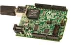
DC2026C-KIT
Analog Devices Inc.
Development Boards & Kits - AVR DC2026C with DC934A Linduino One Isolated Arduino-Compatible Demonstration Board with LTC2607/LTC2422 (DC934A) Demo Board
| Distributor | SKU | Stock | MOQ | 1 | 10 | 50 | 100 | 1,000 | 10,000 |
|---|---|---|---|---|---|---|---|---|---|
| DigiKey | DC2026C-KIT | 40 | 1 | $175.50 | $175.50 | $175.50 | $175.50 | $175.50 | $175.50 |
| Analog Devices Inc | DC2026C-KIT | 0 | $147.12 | $147.12 | $147.12 | $147.12 | $147.12 | $147.12 | |
| Arrow North American Components | DC2026C-KIT | 0 | 1 | $195.76 | $195.76 | $195.76 | $195.76 | $195.76 | $195.76 |
| element14 APAC | DC2026C-KIT | 18 | 1 | * $172.64 | * $172.64 | * $172.64 | * $172.64 | * $172.64 | * $172.64 |
| Farnell | DC2026C-KIT | 14 | 1 | * $170.48 | * $170.48 | * $170.48 | * $170.48 | * $170.48 | * $170.48 |
| Mouser Electronics | DC2026C-KIT | 49 | 1 | $153.03 | $153.03 | $153.03 | $153.03 | $153.03 | $153.03 |
| Newark | DC2026C-KIT | 3 | 1 | $168.62 | $168.62 | $168.62 | $168.62 | $168.62 | $168.62 |
| Verical Marketplace | DC2026C-KIT | 212 | 1 | $145.58 | $148.65 | $144.74 | $142.86 | $141.03 | $141.03 |
| Win Source | DC2026C-KIT | 5150 |
| Distributor | SKU | Stock | MOQ | 1 | 10 | 50 | 100 | 1,000 | 10,000 |
|---|---|---|---|---|---|---|---|---|---|
| DigiKey | OP400GPZ | 3687 | 1 | $20.56 | $16.42 | $15.39 | $14.25 | $13.39 | $13.39 |
| Analog Devices Inc | OP400GPZ | 1079 | 1 | $19.19 | $17.64 | $16.90 | $14.89 | $12.93 | $12.93 |
| Arrow Europe | OP400GPZ | 231 | 1 | $20.36 | $13.37 | $11.01 | $13.11 | $9.09 | $9.09 |
| Arrow North American Components | OP400GPZ | 0 | 50 | $17.02 | $15.51 | $13.10 | $12.43 | $0.00 | $0.00 |
| element14 APAC | OP400GPZ | 17 | 1 | * $24.30 | * $19.41 | * $18.19 | * $16.85 | * $16.21 | * $16.21 |
| Farnell | OP400GPZ | 40 | 1 | * $24.23 | * $20.50 | * $19.66 | * $17.30 | * $16.95 | * $16.95 |
| Mouser Electronics | OP400GPZ | 114 | 1 | $20.00 | $14.83 | $13.36 | $11.65 | $11.16 | $11.16 |
| Newark | OP400GPZ | 51 | 1 | $22.87 | $18.27 | $16.49 | $15.85 | $15.85 | $15.85 |
| Verical Marketplace | OP400GPZ | 231 | 1 | $20.36 | $13.37 | $10.78 | $13.11 | $0.00 | $0.00 |
| Win Source | OP400GPZ | 3290 | 3 | $18.78 | $16.00 | $16.00 | $16.00 | $16.00 |
| Distributor | SKU | Stock | MOQ | 1 | 10 | 50 | 100 | 1,000 | 10,000 |
|---|---|---|---|---|---|---|---|---|---|
| DigiKey | OP470GSZ | 4194 | 1 | $16.48 | $13.08 | $11.75 | $11.69 | $10.35 | $9.18 |
| Analog Devices Inc | OP470GSZ | 0 | $15.07 | $13.85 | $13.28 | $11.70 | $10.41 | $10.41 | |
| Arrow Europe | OP470GSZ | 13 | 1 | $16.94 | $13.44 | $12.08 | $12.08 | $9.37 | $9.32 |
| Arrow North American Components | OP470GSZ | 0 | 47 | $9.79 | $8.81 | $10.12 | $7.41 | $6.33 | $6.33 |
| element14 APAC | OP470GSZ | 138 | 1 | * $18.76 | * $14.88 | * $13.38 | * $13.38 | * $12.28 | * $12.28 |
| Farnell | OP470GSZ | 148 | 1 | * $19.53 | * $15.77 | * $15.12 | * $15.12 | * $13.05 | * $13.05 |
| Mouser Electronics | OP470GSZ | 352 | 1 | $16.59 | $11.98 | $10.11 | $9.12 | $8.76 | $8.76 |
| Newark | OP470GSZ | 138 | 1 | $16.97 | $13.47 | $12.78 | $12.10 | $11.77 | $11.77 |
| Verical Marketplace | OP470GSZ | 13 | 1 | $0.00 | $8.81 | $0.00 | $7.41 | $0.00 | $0.00 |
| Win Source | OP470GSZ | 5463 | 2 | $8.00 | $6.15 | $5.54 | $5.54 | $5.54 |
| Distributor | SKU | Stock | MOQ | 1 | 10 | 50 | 100 | 1,000 | 10,000 |
|---|---|---|---|---|---|---|---|---|---|
| DigiKey | AD215AY | 0 | 1 | $113.14 | $107.30 | $104.38 | $97.08 | $97.08 | $97.08 |
| Analog Devices Inc | AD215AY | 5 | 1 | $118.74 | $112.61 | $109.55 | $109.55 | $109.55 | $109.55 |
| Arrow North American Components | AD215AY | 0 | 1 | $89.18 | $85.80 | $0.00 | $69.45 | $64.67 | $64.67 |
| element14 APAC | AD215AY | 1 | 1 | * $128.80 | * $118.95 | * $113.08 | * $109.15 | * $109.15 | * $109.15 |
| Farnell | AD215AY | 1 | 1 | * $120.85 | * $114.61 | * $111.48 | * $107.06 | * $107.06 | * $107.06 |
| Mouser Electronics | AD215AY | 0 | 1 | $73.83 | |||||
| Newark | AD215AY | 3 | 1 | $0.00 | $0.00 | $0.00 | $0.00 | $0.00 | $0.00 |
| Verical Marketplace | AD215AY | 102 | 1 | $97.88 | $92.52 | $90.05 | $88.87 | $88.87 | $88.87 |
| Win Source | AD215AY | 600 | 1 |
| Distributor | SKU | Stock | MOQ | 1 | 10 | 50 | 100 | 1,000 | 10,000 |
|---|---|---|---|---|---|---|---|---|---|
| DigiKey | AD602ARZ | 0 | 1000 | $85.91 | $71.58 | $68.00 | $64.07 | $58.38 | $58.38 |
| Analog Devices Inc | AD602ARZ | 283 | 1 | $57.03 | $53.58 | $51.85 | $48.92 | $48.92 | $48.92 |
| Arrow Europe | AD602ARZ | 5 | 5 | $42.02 | $55.60 | $37.73 | $34.33 | $34.33 | $34.33 |
| Arrow North American Components | AD602ARZ | 0 | 11 | $35.49 | $34.75 | $34.75 | $34.75 | ||
| element14 APAC | AD602ARZ | 1 | 1 | * $94.95 | * $79.11 | * $75.16 | * $70.81 | * $70.81 | * $70.81 |
| Farnell | AD602ARZ | 1 | 1 | * $89.03 | * $76.28 | * $72.27 | * $70.83 | * $70.83 | * $70.83 |
| Mouser Electronics | AD602ARZ | 386 | 1 | $50.62 | $50.62 | $50.62 | $50.62 | $50.62 | $50.62 |
| Newark | AD602ARZ | 1 | 1 | $85.90 | $71.57 | $66.03 | $66.03 | $66.03 | $66.03 |
| Verical Marketplace | AD602ARZ | 5 | 5 | $46.71 | $55.60 | $48.40 | $48.40 | $48.40 | $48.40 |
| Win Source | AD602ARZ | 7010 | 18 |
| Distributor | SKU | Stock | MOQ | 1 | 10 | 50 | 100 | 1,000 | 10,000 |
|---|---|---|---|---|---|---|---|---|---|
| DigiKey | AD605BRZ | 0 | $35.74 | $29.04 | $26.42 | $26.42 | $24.54 | $24.54 | |
| Analog Devices Inc | AD605BRZ | 0 | $36.17 | $33.36 | $31.86 | $28.49 | $27.17 | $27.17 | |
| Arrow North American Components | AD605BRZ | 0 | 48 | $29.57 | $29.57 | $29.57 | $28.98 | ||
| element14 APAC | AD605BRZ | 3 | 1 | * $40.66 | * $33.05 | * $30.06 | * $30.06 | * $27.93 | * $27.93 |
| Farnell | AD605BRZ | 3 | 1 | * $37.93 | * $33.86 | * $32.32 | * $32.32 | * $28.33 | * $28.33 |
| Mouser Electronics | AD605BRZ | 44 | 1 | $24.90 | $23.71 | $23.02 | $22.87 | $22.87 | $22.87 |
| Newark | AD605BRZ | 3 | 1 | $36.81 | $29.91 | $28.56 | $27.21 | $27.21 | $27.21 |
| Verical Marketplace | AD605BRZ | 16 | 16 | $26.33 | $23.86 | $21.08 | $20.88 | $20.88 | $20.88 |
| Win Source | AD605BRZ | 7000 | 5 |