|
|
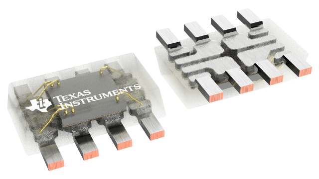
Texas Instruments
OPT4060DTSR
|
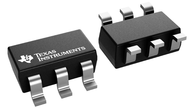
Texas Instruments
TPS3808EG18DBVR
|
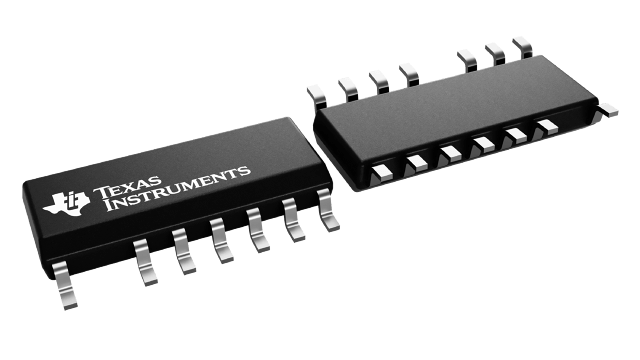
Texas Instruments
UCC256601DDBR
|
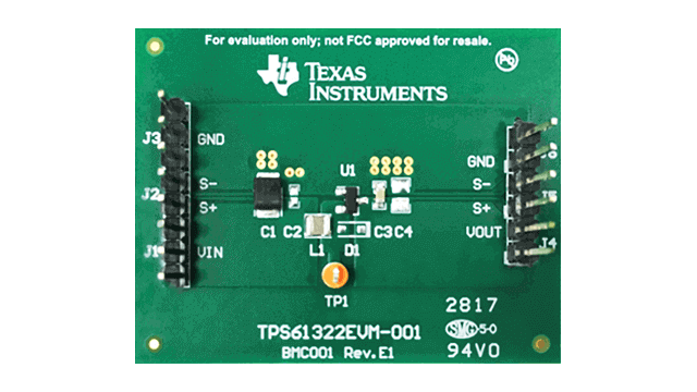
Texas Instruments
TPS61322EVM-001
|
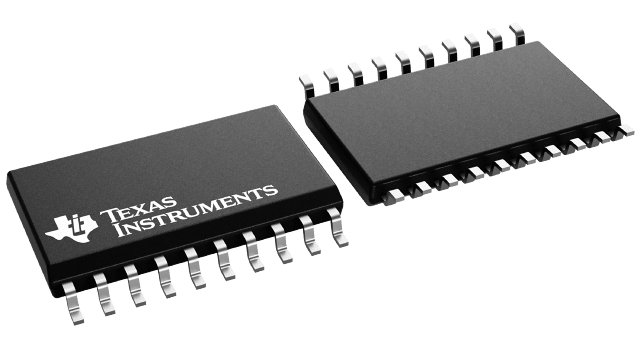
Texas Instruments
SN74LV244BMDWREP
|
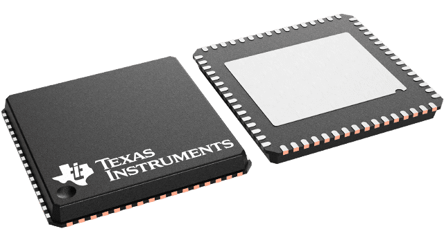
Texas Instruments
ADC32RF54IRTD
|
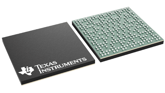
Texas Instruments
AM2431BSDGHIALXR
|

Texas Instruments
AM2432BKEGHIALXR
|

Texas Instruments
AM2432BKFGHIALXR
|
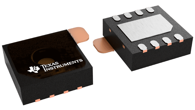
Texas Instruments
HDC3021DEHR
|
| Price |
|
|
|
|
|
|
|
|
|
|
|
| RoHS |
|
Y |
Y |
Y |
|
Y |
Y |
Y |
Y |
Y |
Y |
| Lead Status |
|
Y |
Y |
Y |
|
Y |
Y |
See ti.com |
See ti.com |
See ti.com |
Y |
| Input type |
|
Light |
|
|
|
Standard CMOS |
|
|
|
|
|
| Interface type |
|
I2C |
|
|
|
|
JESD204B |
|
|
|
I2C |
| Operating temperature range(C) |
|
-40 |
-40 |
-40 |
|
-55 |
-40 |
-40 |
-40 |
-40 |
-40 |
| Package area(mm^2) |
|
2.52 |
8.12 |
59.4 |
|
131.84 |
81 |
121 |
121 |
121 |
6.25 |
| Package size (L x W)(mm) |
|
2.1 x 1.2 |
2.9 x 2.8 |
9.9 x 6 |
|
12.8 x 10.3 |
9 x 9 |
11 x 11 |
11 x 11 |
11 x 11 |
2.5 x 2.5 |
| Package type |
|
SOT-5X3 |
SOT-23 |
SOIC |
|
SOIC |
VQFNP |
FCCSP |
FCCSP |
FCCSP |
WSON |
| Pin count |
|
8 |
6 |
14 |
|
20 |
64 |
293 |
293 |
293 |
8 |
| Rating |
|
Catalog |
Catalog |
Catalog |
|
HiRel Enhanced Product |
Catalog |
|
|
|
Catalog |
| TI.com inventory |
|
500 |
8500 |
8645 |
|
1480 |
200 |
5707 |
1881 |
2630 |
17919 |
| Approx. price(US$) |
|
1.23 | 1ku |
.541 | 1ku |
.9 | 1ku |
|
.76 | 1ku |
1490 | 1u |
6.815 | 1ku |
7.231 | 1ku |
9.028 | 1ku |
1.85 | 1ku |
| Features |
|
|
Manual reset capable,Reset time delay,Separate VDD & sense,Undervoltage monitor only |
High frequency,High-voltage startup,Integrated X-cap discharge,Low audible noise,PFC ON/OFF signal,USB C/PD compatible,Wide VIN,Wide VOUT |
|
Balanced outputs,Over-voltage tolerant inputs,Partial power down (Ioff),Very high speed (tpd 5-10ns) |
High Dynamic Range,High Performance,Ultra High Speed |
EtherCAT,EtherNet/IP,IO-Link,Integrated industrial protocols,Profinet,TSN |
EtherCAT,EtherNet/IP,IO-Link,Integrated industrial protocols,Profinet,TSN |
EtherCAT,EtherNet/IP,IO-Link,Integrated industrial protocols,Profinet,TSN |
|
| Iq(typ)(mA) |
|
|
0.0006 |
|
|
|
|
|
|
|
|
| Number of supplies monitored |
|
|
1 |
|
|
|
|
|
|
|
|
| Output driver type/reset output |
|
|
Active-low,Open-drain |
|
|
|
|
|
|
|
|
| Supply voltage(max)(V) |
|
|
6.5 |
|
|
5.5 |
|
|
|
|
5.5 |
| Supply voltage(min)(V) |
|
|
1.7 |
|
|
2 |
|
|
|
|
1.62 |
| TI functional safety category |
|
|
|
|
|
|
|
|
|
|
|
| Threshold voltage 1(typ)(V) |
|
|
1.67,3.08,Adjustable |
|
|
|
|
|
|
|
|
| Time delay(ms) |
|
|
Programmable |
|
|
|
|
|
|
|
|
| Watchdog timer WDI(s) |
|
|
None |
|
|
|
|
|
|
|
|
| Control mode |
|
|
|
Current |
|
|
|
|
|
|
|
| Topology |
|
|
|
Half bridge,LLC |
|
|
|
|
|
|
|
| Vin(max)(V) |
|
|
|
18.5 |
|
|
|
|
|
|
|
| Vin(min)(V) |
|
|
|
9 |
|
|
|
|
|
|
|
| IOH(max)(mA) |
|
|
|
|
|
-12 |
|
|
|
|
|
| IOL(max)(mA) |
|
|
|
|
|
12 |
|
|
|
|
|
| Number of channels |
|
|
|
|
|
8 |
|
|
|
|
|
| Output type |
|
|
|
|
|
3-State |
|
|
|
|
|
| Supply current(max)(A) |
|
|
|
|
|
20 |
|
|
|
|
|
| Technology family |
|
|
|
|
|
LV-A |
|
|
|
|
|
| Analog input BW(MHz) |
|
|
|
|
|
|
2300 |
|
|
|
|
| ENOB(bit) |
|
|
|
|
|
|
10.5 |
|
|
|
|
| Input buffer |
|
|
|
|
|
|
Yes |
|
|
|
|
| Number of input channels |
|
|
|
|
|
|
2 |
|
|
|
|
| Peak-to-peak input voltage range(V) |
|
|
|
|
|
|
1.1 |
|
|
|
|
| Power consumption(typ)(mW) |
|
|
|
|
|
|
3400 |
|
|
|
|
| Resolution(Bits) |
|
|
|
|
|
|
14 |
|
|
|
|
| SFDR(dB) |
|
|
|
|
|
|
75 |
|
|
|
|
| SNR(dB) |
|
|
|
|
|
|
65.5 |
|
|
|
|
| Sample rate(max)(Msps) |
|
|
|
|
|
|
2600 |
|
|
|
|
| ADC type |
|
|
|
|
|
|
|
12-bit SAR |
12-bit SAR |
12-bit SAR |
|
| CAN(#) |
|
|
|
|
|
|
|
2 |
2 |
2 |
|
| Communication interface |
|
|
|
|
|
|
|
ADC,CAN-FD,Ethernet,GPIO,I2C,QSPI,SD/SDIO,UART,USB,eCAP,ePWM,eQEP |
ADC,CAN-FD,Ethernet,GPIO,I2C,QSPI,SD/SDIO,UART,USB,eCAP,ePWM,eQEP |
ADC,CAN-FD,Ethernet,GPIO,I2C,QSPI,SD/SDIO,UART,USB,eCAP,ePWM,eQEP |
|
| Ethernet |
|
|
|
|
|
|
|
Yes |
Yes |
Yes |
|
| Frequency(MHz) |
|
|
|
|
|
|
|
800 |
800 |
800 |
|
| Number of GPIOs |
|
|
|
|
|
|
|
148,198 |
148,198 |
148,198 |
|
| PWM(Ch) |
|
|
|
|
|
|
|
6,9 |
6,9 |
6,9 |
|
| Power supply solution |
|
|
|
|
|
|
|
LP8733,TPS65219 |
LP8733,TPS65219 |
LP8733,TPS65219 |
|
| RAM(kByte) |
|
|
|
|
|
|
|
2000 |
2000 |
2000 |
|
| SPI |
|
|
|
|
|
|
|
4,5 |
4,5 |
4,5 |
|
| UART |
|
|
|
|
|
|
|
7,9 |
7,9 |
7,9 |
|
| USB |
|
|
|
|
|
|
|
USB 2.0,USB 3.1 |
USB 2.0,USB 3.1 |
USB 2.0,USB 3.1 |
|
| Average supply current(typ)(A) |
|
|
|
|
|
|
|
|
|
|
0.0000004 |
| Relative humidity accuracy(typ)(%RH) |
|
|
|
|
|
|
|
|
|
|
0.5 |
| Relative humidity operating range(typ)(%RH) |
|
|
|
|
|
|
|
|
|
|
0 to 100 |
| Temperature accuracy(typ)(C) |
|
|
|
|
|
|
|
|
|
|
0.1 |