|
|
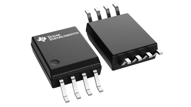
Texas Instruments
AMC1311QDWVRQ1
|
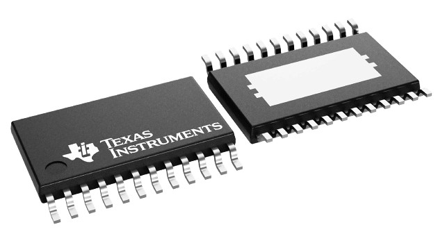
Texas Instruments
DRV10975ZRHFR
|
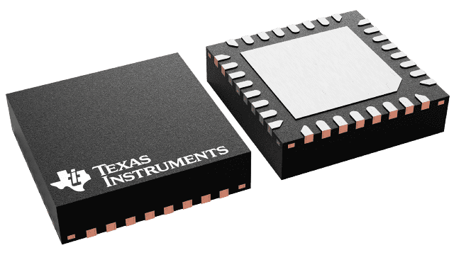
Texas Instruments
MSP430FR2153TRHAT
|

Texas Instruments
MSP430FR2155TPT
|

Texas Instruments
MSP430FR2355TRHAT
|
Texas Instruments
PTPS65987DDHRSHT
|
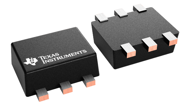
Texas Instruments
TLV62569ADRLR
|
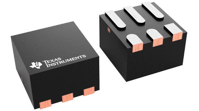
Texas Instruments
TPS6282518DMQR
|

Texas Instruments
TPS6282518DMQT
|

Texas Instruments
TPS62825DMQT
|
| Price |
|
|
|
|
|
|
|
|
|
|
|
| RoHS |
|
Y |
Y |
Compliant |
Compliant |
Compliant |
See ti.com |
Y |
Y |
Y |
Y |
| Lead Status |
|
Y |
See ti.com |
No |
No |
No |
See ti.com |
See ti.com |
Y |
Y |
Y |
| Package Group |
|
SOIC|8 |
HTSSOP|24,VQFN|24 |
LQFP|48,TSSOP|38,VQFN|40 |
LQFP|48,TSSOP|38,VQFN|40 |
LQFP|48,TSSOP|38,VQFN|40 |
VQFN |
SOT-5X3|6 |
VSON-HR|6 |
VSON-HR|6 |
VSON-HR|6 |
| Input range(Vp-p) |
|
2 |
|
|
|
|
|
|
|
|
|
| Gain error drift (+/-)(Typ)(ppm/C) |
|
30,5 |
|
|
|
|
|
|
|
|
|
| Rating |
|
Automotive |
Catalog |
Catalog |
Catalog |
Catalog |
Catalog |
Catalog |
Catalog |
Catalog |
Catalog |
| Input offset (+/-)(Max)(mV) |
|
9.9,1.5 |
|
|
|
|
|
|
|
|
|
| Gain error (+/-)(Max)(%) |
|
1,0.3 |
|
|
|
|
|
|
|
|
|
| CMTI(Min)(kV/s) |
|
15,75 |
|
|
|
|
|
|
|
|
|
| Isolation working voltage VIOWM (rms)(V) |
|
1500 |
|
|
|
|
|
|
|
|
|
| Gain non-linearity (+/-)(Max)(%) |
|
0.04 |
|
|
|
|
|
|
|
|
|
| Small signal bandwidth(Typ)(kHz) |
|
220,275 |
|
|
|
|
|
|
|
|
|
| Input offset drift (+/-)(Typ)(uV/C) |
|
20,3 |
|
|
|
|
|
|
|
|
|
| Operating temperature range(C) |
|
-40 to 125 |
-40 to 125 |
|
-40 to 105 |
-40 to 105 |
|
-40 to 125 |
-40 to 125 |
-40 to 125 |
-40 to 125 |
| Package size |
|
mm2 |
|
|
mm2 |
mm2 |
|
mm2 |
mm2 |
mm2 |
mm2 |
| Isolation transient overvoltage VIOTM (peak)(V) |
|
7000 |
|
|
|
|
|
|
|
|
|
| Approx. price(US$) |
|
3.13 | 1ku |
1.05 | 1ku |
|
1.60 | 1ku |
2.40 | 1ku |
|
0.44 | 1ku |
.431 | 1ku |
.41 | 1ku |
0.52 | 1ku |
| Control I/F |
|
|
1xPWM,Analog,Serial |
|
|
|
|
|
|
|
|
| Peak output current(A) |
|
|
3 |
|
|
|
|
|
|
|
|
| Sensor type |
|
|
Sensorless |
|
|
|
|
|
|
|
|
| Control method |
|
|
Sinusoidal Control |
|
|
|
|
|
|
|
|
| Architecture |
|
|
Integrated FET |
|
|
|
|
|
|
|
|
| Features |
|
|
Buck Step Down Converter,Initial Position Detect (IPD),Rotor Lock Protection,SPI/I2C,Integrated Motor Control,Integrated FETs,Tach/FG Feedback |
Real-Time Clock |
Real-Time Clock |
DAC,OpAmp,PGA,Real-Time Clock |
|
Enable,Forced PWM,Power Good,Synchronous Rectification |
Enable,Light Load Efficiency,Output Discharge,Over Current Protection,Power Good,Pre-Bias Start-Up,Synchronous Rectification |
Enable,Light Load Efficiency,Output Discharge,Over Current Protection,Power Good,Pre-Bias Start-Up,Synchronous Rectification |
Enable,Light Load Efficiency,Output Discharge,Over Current Protection,Power Good,Pre-Bias Start-Up,Synchronous Rectification |
| RDS(ON) (HS + LS)(mOhms) |
|
|
250 |
|
|
|
|
|
|
|
|
| Vs(Max)(V) |
|
|
18 |
|
|
|
|
|
|
|
|
| Vs ABS(Max)(V) |
|
|
23 |
|
|
|
|
|
|
|
|
| Vs(Min)(V) |
|
|
6.5 |
|
|
|
|
|
|
|
|
| I2C |
|
|
|
2 |
2 |
2 |
|
|
|
|
|
| Comparator Channels (#) |
|
|
|
2 |
|
|
|
|
|
|
|
| ADC |
|
|
|
Channels(#) |
12-bit SAR |
12-bit SAR |
|
|
|
|
|
| RAM(KB) |
|
|
|
2 |
4 |
4 |
|
|
|
|
|
| Timers - 16-bit |
|
|
|
4 |
4 |
4 |
|
|
|
|
|
| Bootloader (BSL) |
|
|
|
UART |
UART |
UART |
|
|
|
|
|
| Approx. Price (US$) |
|
|
|
1.25 | 1ku |
|
|
1.99 | 1ku |
|
|
|
|
| Operating Temperature Range(C) |
|
|
|
-40 to 105 |
|
|
-40 to 85 |
|
|
|
|
| Package Size |
|
|
|
mm2 |
|
|
|
|
|
|
|
| GPIO Pins(#) |
|
|
|
44 |
|
|
|
|
|
|
|
| Non-volatile Memory (KB) |
|
|
|
16 |
|
|
|
|
|
|
|
| Special I/O |
|
|
|
N/A |
N/A |
N/A |
|
|
|
|
|
| SPI |
|
|
|
4 |
4 |
4 |
|
|
|
|
|
| USB |
|
|
|
No |
No |
No |
|
|
|
|
|
| UART |
|
|
|
2 |
2 |
2 |
|
|
|
|
|
| Non-volatile memory (kB) |
|
|
|
|
32 |
32 |
|
|
|
|
|
| GPIO pins(#) |
|
|
|
|
44 |
44 |
|
|
|
|
|
| Comparator channels (#) |
|
|
|
|
2 |
2 |
|
|
|
|
|
| External Power Path Control |
|
|
|
|
|
|
GPIO,I2C |
|
|
|
|
| Data Role |
|
|
|
|
|
|
DFP,DRD,DRP,UFP |
|
|
|
|
| USB Speed(Mbps) |
|
|
|
|
|
|
N/A |
|
|
|
|
| Iq(Typ)(uA) |
|
|
|
|
|
|
45 |
|
4 |
4 |
|
| Alternate Mode |
|
|
|
|
|
|
Yes |
|
|
|
|
| Realtime VBUS monitoring |
|
|
|
|
|
|
Yes |
|
|
|
|
| Configuration |
|
|
|
|
|
|
N/A |
|
|
|
|
| Function |
|
|
|
|
|
|
PD Controller |
|
|
|
|
| Dead Battery Support |
|
|
|
|
|
|
Yes |
|
|
|
|
| Power Role |
|
|
|
|
|
|
DRP,Sink,Source |
|
|
|
|
| Policy Manager |
|
|
|
|
|
|
Integrated |
|
|
|
|
| Internal Power Path |
|
|
|
|
|
|
20V 5A Source/Sink,5V 600mA VCONN |
|
|
|
|
| Iout(Max)(A) |
|
|
|
|
|
|
|
2 |
2 |
2 |
2 |
| Iq(Typ)(mA) |
|
|
|
|
|
|
|
0.035 |
|
|
0.004 |
| Vout(Max)(V) |
|
|
|
|
|
|
|
5.5 |
4 |
4 |
4 |
| Switching frequency(Min)(kHz) |
|
|
|
|
|
|
|
1500 |
2200 |
2200 |
2200 |
| Vin(Max)(V) |
|
|
|
|
|
|
|
5.5 |
5.5 |
5.5 |
5.5 |
| Type |
|
|
|
|
|
|
|
Converter |
Converter |
Converter |
Converter |
| Duty cycle(Max)(%) |
|
|
|
|
|
|
|
100 |
100 |
100 |
100 |
| Switching frequency(Max)(kHz) |
|
|
|
|
|
|
|
1500 |
2200 |
2200 |
2200 |
| Regulated outputs(#) |
|
|
|
|
|
|
|
1 |
1 |
1 |
1 |
| Vout(Min)(V) |
|
|
|
|
|
|
|
0.6 |
0.6 |
0.6 |
0.6 |
| Vin(Min)(V) |
|
|
|
|
|
|
|
2.5 |
2.4 |
2.4 |
2.4 |
| Control mode |
|
|
|
|
|
|
|
Constant on-time (COT) |
Constant on-time (COT),DCS-Control |
Constant on-time (COT),DCS-Control |
Constant on-time (COT),DCS-Control |
| TI.com inventory |
|
|
|
|
|
|
|
|
0 |
0 |
|
| Switching frequency(Typ)(kHz) |
|
|
|
|
|
|
|
|
|
|
2200 |