|
|
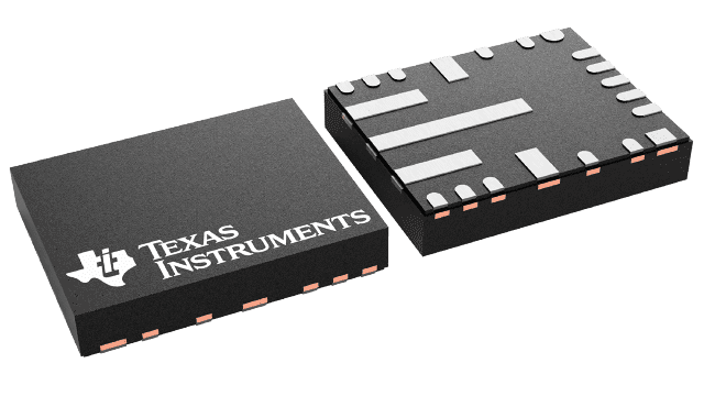
Texas Instruments
LMS3635LQRNLTQ1
|
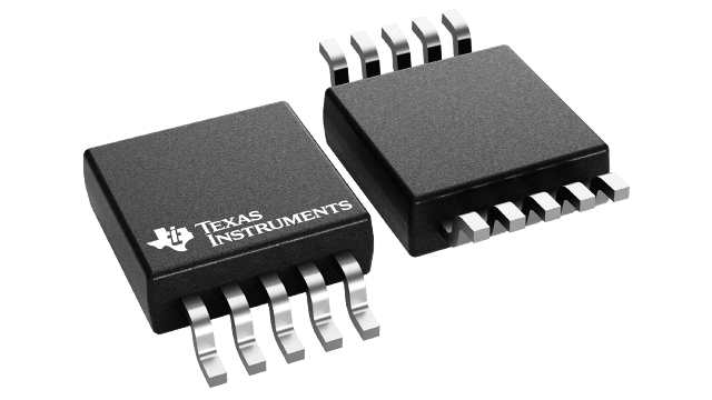
Texas Instruments
THVD1512DGS
|
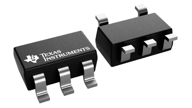
Texas Instruments
TLV70325DBVR
|
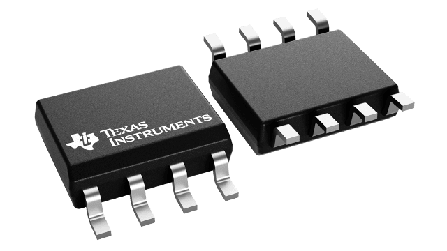
Texas Instruments
OPA2189IDGKR
|
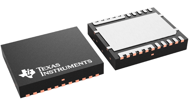
Texas Instruments
CSD95491Q5MCT
|
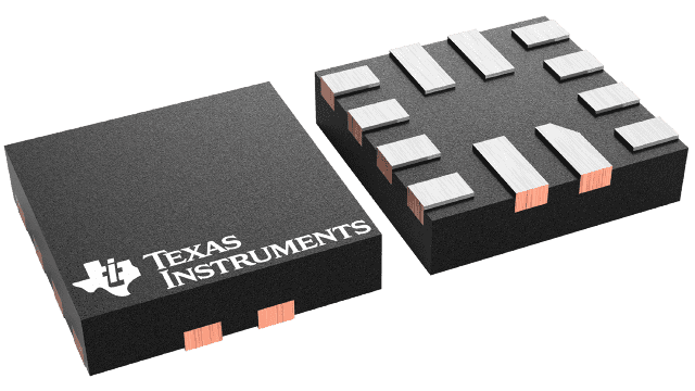
Texas Instruments
TUSB212RWBT
|

Texas Instruments
UCC24612-1DBVR
|
Texas Instruments
PS7A5401QRGRRQ1
|
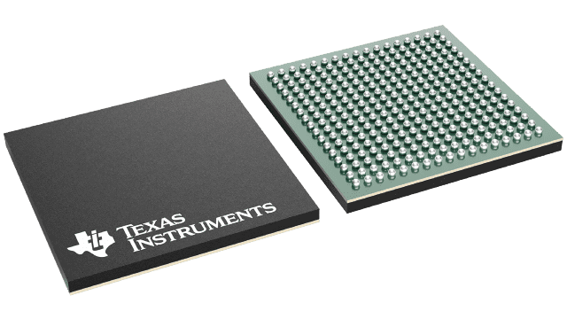
Texas Instruments
AFE58JD28ZAV
|
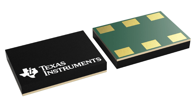
Texas Instruments
LMK61E0-155M52SIAR
|
| Price |
|
|
|
|
|
|
|
|
|
|
|
| RoHS |
|
Compliant |
Compliant |
Y |
See ti.com |
Y |
Y |
Compliant |
See ti.com |
Compliant |
Compliant |
| Lead Status |
|
No |
No |
Y |
See ti.com |
Y |
Y |
No |
See ti.com |
No |
No |
| Switching Frequency(Min)(kHz) |
|
250 |
|
|
|
|
|
|
|
|
|
| Package Group |
|
VQFN-HR |
SOIC,VSSOP |
|
SOIC|8,VSSOP|8 |
VSON-CLIP|12 |
X2QFN|12 |
SOT-23 |
VQFN |
NFBGA |
|
| Control Mode |
|
Current Mode |
|
|
|
|
|
|
|
|
|
| Switching Frequency(Max)(kHz) |
|
500 |
|
|
|
|
|
|
|
|
|
| Duty Cycle(Max)(%) |
|
98 |
|
|
|
|
|
|
|
|
|
| Rating |
|
Automotive |
Catalog |
Catalog |
Catalog |
|
Catalog |
Catalog |
Automotive |
Catalog |
Catalog |
| Type |
|
Converter |
|
|
|
|
|
|
|
|
|
| Operating Temperature Range(C) |
|
-40 to 150 |
-40 to 125 |
|
-40 to 125 |
|
|
-40 to 125 |
-40 to 140 |
-40 to 85 |
|
| Regulated Outputs(#) |
|
1 |
|
|
|
|
|
|
1 |
|
|
| Vout(Max)(V) |
|
15 |
|
|
|
|
|
|
5.1 |
|
|
| Vin(Max)(V) |
|
42 |
|
|
|
|
|
|
6.5 |
|
|
| Iq(Typ)(mA) |
|
0.015 |
|
|
|
|
|
|
3 |
|
|
| Vout(Min)(V) |
|
1 |
|
|
|
|
|
|
0.8 |
|
|
| Features |
|
Enable,Frequency Synchronization,Light Load Efficiency,Power Good,Pre-Bias Start-Up,Synchronous Rectification |
|
Enable |
EMI Hardened,High Cload Drive,Zero Drift |
|
USB 2.0 Redriver with 4 Meter Cable Redriving Strength |
|
Enable,Foldback Overcurrent Protection,Output Discharge,Power Good,Soft Start |
Analog Front End (AFE) |
Standard,7x5mm |
| Vin(Min)(V) |
|
3.5 |
|
|
|
|
|
|
1.1 |
|
|
| Approx. Price (US$) |
|
2.83 | 1ku |
0.95 | 1ku |
|
|
|
|
0.40 | 1ku |
3.78 | 1ku |
172.55 | 1ku |
|
| Iout(Max)(A) |
|
3.5 |
|
|
|
|
|
|
4 |
|
|
| Signaling Rate(Max)(Mbps) |
|
|
0.5 |
|
|
|
|
|
|
|
|
| IEC 61000-4-2 Contact(+/- kV) |
|
|
18 |
|
|
|
|
|
|
|
|
| HBM ESD(kV) |
|
|
30 |
|
|
|
|
|
|
|
|
| Duplex |
|
|
Full |
|
|
|
|
|
|
|
|
| Isolated |
|
|
No |
|
|
|
|
|
|
|
|
| Supply Voltage(s)(Nom)(V) |
|
|
5 |
|
|
|
|
|
|
|
|
| Fault Protection(V) |
|
|
-18 to |
|
|
|
|
|
|
|
|
| Common Mode Range |
|
|
-15 to |
|
|
|
|
|
|
|
|
| No. of RX |
|
|
1 |
|
|
|
|
|
|
|
|
| Number of Nodes |
|
|
256 |
|
|
|
|
|
|
|
|
| No. of TX |
|
|
1 |
|
|
|
|
|
|
|
|
| ICC(Max)(mA) |
|
|
1 |
|
|
|
|
|
|
|
|
| Accuracy(%) |
|
|
|
2 |
|
|
|
|
1 |
|
|
| Dropout voltage (Vdo)(typ)(mV) |
|
|
|
220 |
|
|
|
|
|
|
|
| Fixed output options(V) |
|
|
|
2.5 |
|
|
|
|
|
|
|
| Iout(max)(A) |
|
|
|
0.3 |
|
|
|
|
|
|
|
| Iq(typ)(mA) |
|
|
|
0.035 |
|
|
|
|
|
|
|
| Load capacitance(min)(F) |
|
|
|
0.1 |
|
|
|
|
|
|
|
| Maximum package height(mm) |
|
|
|
1.45 |
|
|
|
|
|
|
|
| Noise(Vrms) |
|
|
|
48 |
|
|
|
|
|
|
|
| Operating temperature range(C) |
|
|
|
-40 |
|
-55 to 150 |
-40 to 85,0 to 70 |
|
|
|
-40 to 85 |
| Output options |
|
|
|
Fixed Output |
|
|
|
|
|
|
|
| PSRR at 100 KHz(dB) |
|
|
|
52 |
|
|
|
|
|
|
|
| Package area(mm^2) |
|
|
|
8.12 |
|
|
|
|
|
|
|
| Package size (L x W)(mm) |
|
|
|
2.9 x 2.8 |
|
|
|
|
|
|
|
| Package type |
|
|
|
SOT-23 |
|
|
|
|
|
|
|
| Pin count |
|
|
|
5.0 |
|
|
|
|
|
|
|
| Regulated outputs(#) |
|
|
|
1 |
|
|
|
|
|
|
|
| TI functional safety category |
|
|
|
|
|
|
|
|
|
|
|
| Thermal resistance JA(C/W) |
|
|
|
254.1 |
|
|
|
|
|
|
|
| Vin(max)(V) |
|
|
|
5.5 |
|
|
|
|
|
|
|
| Vin(min)(V) |
|
|
|
2 |
|
|
|
|
|
|
|
| Vout(max)(V) |
|
|
|
3.3 |
|
|
|
|
|
|
|
| Vout(min)(V) |
|
|
|
1 |
|
|
|
|
|
|
|
| TI.com inventory |
|
|
|
296632 |
|
|
|
|
|
|
|
| Approx. price(US$) |
|
|
|
.042 | 1ku |
|
1.96 | 1ku |
1.45 | 1ku |
|
|
|
4.10 | 1ku |
| Offset Drift(Typ)(uV/C) |
|
|
|
|
0.005 |
|
|
|
|
|
|
| Output Current(Typ)(mA) |
|
|
|
|
65 |
|
|
|
|
|
|
| Package Size |
|
|
|
|
mm2 |
|
|
mm2 |
mm2 |
mm2 |
|
| Total Supply Voltage(Min)(+5V=5, +/-5V=10) |
|
|
|
|
4.5 |
|
|
|
|
|
|
| Architecture |
|
|
|
|
CMOS |
|
|
|
|
|
|
| Slew Rate(Typ)(V/us) |
|
|
|
|
20 |
|
|
|
|
|
|
| Number of Channels(#) |
|
|
|
|
2 |
|
|
|
|
|
|
| Iq per channel(Typ)(mA) |
|
|
|
|
1.3 |
|
|
|
|
|
|
| Vos (Offset Voltage @ 25C)(Max)(mV) |
|
|
|
|
0.005 |
|
|
|
|
|
|
| Total Supply Voltage(Max)(+5V=5, +/-5V=10) |
|
|
|
|
36 |
|
|
|
|
|
|
| GBW(Typ)(MHz) |
|
|
|
|
14 |
|
|
|
|
|
|
| Vn at 1kHz(Typ)(nV/rtHz) |
|
|
|
|
5.2 |
|
|
|
|
|
|
| CMRR(Typ)(dB) |
|
|
|
|
168 |
|
|
|
|
|
|
| Input Bias Current(Max)(pA) |
|
|
|
|
300 |
|
|
|
|
|
|
| Rail-to-Rail |
|
|
|
|
In to V-,Out |
|
|
|
|
|
|
| Iq per channel(Max)(mA) |
|
|
|
|
1.7 |
|
|
|
|
|
|
| ID, continuous drain current at Ta=25degC(A) |
|
|
|
|
|
60 |
|
|
|
|
|
| Configuration |
|
|
|
|
|
PowerStage |
|
|
|
|
|
| Ploss current(A) |
|
|
|
|
|
30 |
|
|
|
|
|
| VDS(V) |
|
|
|
|
|
20 |
|
|
|
|
|
| Package size |
|
|
|
|
|
mm2 |
mm2 |
|
|
|
|
| Power loss(W) |
|
|
|
|
|
2.6 |
|
|
|
|
|
| Package (mm) |
|
|
|
|
|
SON5x6 DualCool PowerStage |
|
|
|
|
|
| ICC(Typ)(uA) |
|
|
|
|
|
|
22mA |
|
|
|
|
| ICC(Max)(uA) |
|
|
|
|
|
|
30mA |
|
|
|
|
| Number of channels(#) |
|
|
|
|
|
|
1 |
|
|
|
|
| Input/ouput voltage(Max)(V) |
|
|
|
|
|
|
3.6 |
|
|
|
|
| Device type |
|
|
|
|
|
|
Redriver |
|
|
|
|
| VCC(Min)(V) |
|
|
|
|
|
|
3 |
|
|
|
|
| Bandwidth(MHz) |
|
|
|
|
|
|
240 |
|
|
|
|
| ESD HBM(kV) |
|
|
|
|
|
|
2 |
|
|
|
|
| Input/ouput voltage(Min)(V) |
|
|
|
|
|
|
0 |
|
|
|
|
| USB speed(Mbps) |
|
|
|
|
|
|
480 |
|
|
|
|
| ESD HBM(Typ)(kV) |
|
|
|
|
|
|
2 |
|
|
|
|
| Function |
|
|
|
|
|
|
USB2 |
|
|
|
|
| VCC(Max)(V) |
|
|
|
|
|
|
3.6 |
|
|
|
|
| Frequency(Max)(kHz) |
|
|
|
|
|
|
|
1000 |
|
|
|
| UVLO Thresholds On/Off(V) |
|
|
|
|
|
|
|
4.5/4 |
|
|
|
| Output Options |
|
|
|
|
|
|
|
|
Adjustable Output |
|
|
| Thermal Resistance JA(C/W) |
|
|
|
|
|
|
|
|
40 |
|
|
| Noise(uVrms) |
|
|
|
|
|
|
|
|
4.4 |
|
|
| PSRR @ 100KHz(dB) |
|
|
|
|
|
|
|
|
33 |
|
|
| Output Capacitor Type |
|
|
|
|
|
|
|
|
Ceramic |
|
|
| Vdo(Typ)(mV) |
|
|
|
|
|
|
|
|
150 |
|
|
| Active Supply Current(Typ)(mA) |
|
|
|
|
|
|
|
|
|
260 |
|
| Supply Voltage(Max) |
|
|
|
|
|
|
|
|
|
3.6 |
|
| # Input Channels |
|
|
|
|
|
|
|
|
|
16 |
|
| Interface |
|
|
|
|
|
|
|
|
|
JESD,LVDS |
|
| Supply Voltage(Min) |
|
|
|
|
|
|
|
|
|
3.15 |
|
| Stability(ppm) |
|
|
|
|
|
|
|
|
|
|
25 |
| Jitter(ps) |
|
|
|
|
|
|
|
|
|
|
0.15 |
| Pin/package |
|
|
|
|
|
|
|
|
|
|
6QFM |
| Output frequency(Max)(MHz) |
|
|
|
|
|
|
|
|
|
|
155.52 |
| VCC core(V) |
|
|
|
|
|
|
|
|
|
|
3.3 |
| Output level |
|
|
|
|
|
|
|
|
|
|
LVPECL |