|
|
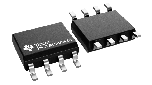
Texas Instruments
TPS7133QD
|
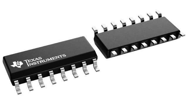
Texas Instruments
SN75LVDS32D
|

Texas Instruments
INA133U
|

Texas Instruments
SN74LVC139ADBR
|

Texas Instruments
OPA2342UA
|
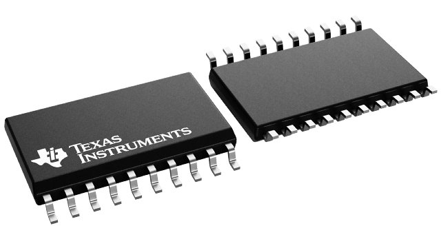
Texas Instruments
SN75LBC172DW
|
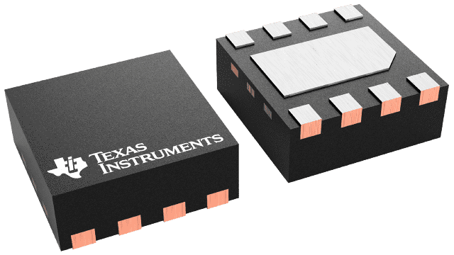
Texas Instruments
BQ24380DSGT
|
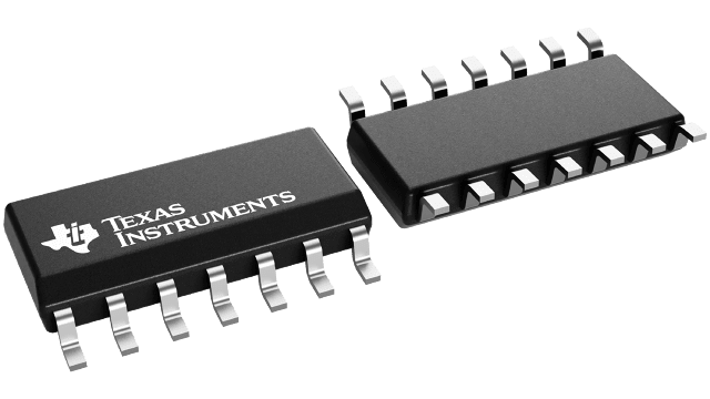
Texas Instruments
TL074IN
|

Texas Instruments
UC3843ADTRG4
|
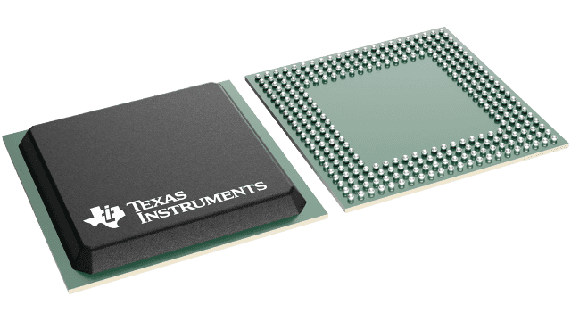
Texas Instruments
TMS320C6413GTSA500
|
| Price |
|
$2.95 |
|
|
$0.24 |
$1.31 |
$3.74 |
|
|
$0.47 |
$46.36 |
| RoHS |
|
Yes |
Yes |
Yes |
Yes |
Yes |
Yes |
Yes |
Compliant |
Compliant |
No |
| Lead Status |
|
Yes |
Yes |
Yes |
Yes |
Yes |
Yes |
Yes |
Yes |
No |
No |
| Fixed Output Options(V) |
|
3.3,4.8,5 |
|
|
|
|
|
|
|
|
|
| Iout(Max)(A) |
|
0.5 |
|
|
|
|
|
|
|
|
|
| Rating |
|
Catalog |
Catalog |
Catalog |
Catalog |
Catalog |
Catalog |
Catalog |
Catalog |
Military |
|
| Operating Temperature Range(C) |
|
-40 to 125 |
0 to 70 |
-40 to 85 |
-40 to 85 |
-40 to 85 |
0 to 70 |
|
-40 to 85,0 to 70 |
0 to 70 |
|
| Accuracy(%) |
|
3 |
|
|
|
|
|
|
|
|
|
| Vin(Max)(V) |
|
10 |
|
|
|
|
|
30 |
|
30 |
|
| Regulated Outputs(#) |
|
1 |
|
|
|
|
|
|
|
|
|
| Iq(Typ)(mA) |
|
0.28 |
|
0.95 |
|
|
|
|
|
|
|
| Package Group |
|
PDIP,SOIC,TSSOP |
TSSOP,SOIC |
SOIC |
BGA MICROSTAR JUNIOR,SO,SOIC,SSOP,TSSOP,TVSOP,VQFN |
SOIC,VSSOP |
PDIP,SOIC |
WSON |
PDIP,SO,SOIC,TSSOP |
PDIP,SOIC,WAFERSALE |
|
| Vout(Max)(V) |
|
9.75 |
|
|
|
|
|
|
|
|
|
| Approx. Price (US$) |
|
1.05 | 1ku |
1.35 | 1ku |
1.15 | 1ku |
0.12 | 1ku |
0.61 | 1ku |
1.89 | 1ku |
0.25 | 1ku |
0.14 | 1ku |
|
|
| Vout(Min)(V) |
|
1.2 |
|
|
|
|
|
|
|
|
|
| Additional Features |
|
Enable,Overcurrent Protection,Power Good,Thermal Shutdown |
|
|
|
N/A |
|
|
N/A |
|
|
| Output Capacitor Type |
|
Non-Ceramic |
|
|
|
|
|
|
|
|
|
| Vin(Min)(V) |
|
2.5 |
|
|
|
|
|
|
|
7.6 |
|
| Output Options |
|
Adjustable Output,Fixed Output |
|
|
|
|
|
|
|
|
|
| Package Size |
|
mm2 |
mm2 |
mm2 |
mm2 |
mm2 |
mm2 |
|
mm2 |
mm2 |
|
| Vdo(Typ)(mV) |
|
235 |
|
|
|
|
|
|
|
|
|
| No. of Tx |
|
|
0 |
|
|
|
|
|
|
|
|
| Output Signal |
|
|
LVTTL |
|
|
|
|
|
|
|
|
| Function |
|
|
Receiver |
|
Decoder/Demultiplexer |
|
|
Charger Front-End Protection |
|
|
|
| Input Signal |
|
|
LVDS |
|
|
|
|
|
|
|
|
| Signaling Rate(Mbps) |
|
|
155 |
|
|
|
|
|
|
|
|
| ESD HBM(kV) |
|
|
8 |
|
2 |
|
|
|
|
|
|
| ICC(Max)(mA) |
|
|
18 |
|
|
|
7 |
|
|
|
|
| No. of Rx |
|
|
4 |
|
|
|
|
|
|
|
|
| Vs(Max)(V) |
|
|
|
36 |
|
|
|
|
|
|
|
| Gain Drift(Max)(ppm/C) |
|
|
|
1 |
|
|
|
|
|
|
|
| Input Offset (+/-)(Max)(uV) |
|
|
|
450 |
|
|
|
|
|
|
|
| Gain(Max)(V/V) |
|
|
|
1 |
|
|
|
|
|
|
|
| Gain Error (+/-)(Max)(%) |
|
|
|
0.05 |
|
|
|
|
|
|
|
| Small Signal Bandwidth(Typ)(MHz) |
|
|
|
1.5 |
|
|
|
|
|
|
|
| Gain(Min)(V/V) |
|
|
|
1 |
|
|
|
|
|
|
|
| Gain(V/V) |
|
|
|
1 |
|
|
|
|
|
|
|
| Common Mode Input High(Min)(V) |
|
|
|
27 |
|
|
|
|
|
|
|
| Common Mode Input Low(Min)(V) |
|
|
|
-27 |
|
|
|
|
|
|
|
| Number of Channels(#) |
|
|
|
1 |
|
2 |
|
|
4 |
|
|
| Vs(Min)(V) |
|
|
|
4.5 |
|
|
|
|
|
|
|
| Input Offset Drift (+/-)(Max)(uV/C) |
|
|
|
5 |
|
|
|
|
|
|
|
| CMRR(Min)(dB) |
|
|
|
80 |
|
76 |
|
|
70 |
|
|
| Slew Rate(Typ)(V/us) |
|
|
|
5 |
|
1 |
|
|
13 |
|
|
| Technology Family |
|
|
|
|
LVC |
|
|
|
|
|
|
| tpd @ Nom Voltage(Max)(ns) |
|
|
|
|
20.6,9.3,7.3,6.2 |
|
|
|
|
|
|
| Output Drive (IOL/IOH)(Max)(mA) |
|
|
|
|
24/-24 |
|
|
|
|
|
|
| Schmitt Trigger |
|
|
|
|
No |
|
|
|
|
|
|
| Configuration |
|
|
|
|
2 |
|
|
|
|
|
|
| Bits(#) |
|
|
|
|
4 |
|
|
|
|
|
|
| Bandwidth(MHz) |
|
|
|
|
100 |
|
|
|
|
|
|
| ICC @ Nom Voltage(Max)(mA) |
|
|
|
|
0.01 |
|
|
|
|
|
|
| F @ Nom Voltage(Max)(Mhz) |
|
|
|
|
100 |
|
|
|
|
|
|
| Type |
|
|
|
|
Standard |
|
|
|
|
|
|
| Channels(#) |
|
|
|
|
2 |
|
|
|
|
|
|
| ESD Charged Device Model(kV) |
|
|
|
|
0.75 |
|
|
|
|
|
|
| Voltage(Nom)(V) |
|
|
|
|
1.8,2.5,2.7,3.3 |
|
|
|
|
|
|
| VCC(Min)(V) |
|
|
|
|
1.65 |
|
|
|
|
|
|
| VCC(Max)(V) |
|
|
|
|
3.6 |
|
|
|
|
|
|
| Digital input leakage(Max)(uA) |
|
|
|
|
5 |
|
|
|
|
|
|
| GBW(Typ)(MHz) |
|
|
|
|
|
1 |
|
|
3 |
|
|
| Output Current(Typ)(mA) |
|
|
|
|
|
15 |
|
|
10 |
|
|
| CMRR(Typ)(dB) |
|
|
|
|
|
88 |
|
|
100 |
|
|
| Iq per channel(Max)(mA) |
|
|
|
|
|
0.25 |
|
|
2.5 |
|
|
| Architecture |
|
|
|
|
|
CMOS |
|
|
FET |
|
|
| Rail-to-Rail |
|
|
|
|
|
In,Out |
|
|
In to V+ |
|
|
| Iq per channel(Typ)(mA) |
|
|
|
|
|
0.15 |
|
|
1.4 |
|
|
| Total Supply Voltage(Max)(+5V=5, +/-5V=10) |
|
|
|
|
|
5.5 |
|
|
36 |
|
|
| Total Supply Voltage(Min)(+5V=5, +/-5V=10) |
|
|
|
|
|
2.7 |
|
|
7 |
|
|
| Offset Drift(Typ)(uV/C) |
|
|
|
|
|
3 |
|
|
18 |
|
|
| Vn at 1kHz(Typ)(nV/rtHz) |
|
|
|
|
|
30 |
|
|
18 |
|
|
| Vos (Offset Voltage @ 25C)(Max)(mV) |
|
|
|
|
|
6 |
|
|
6 |
|
|
| Input Bias Current(Max)(pA) |
|
|
|
|
|
10 |
|
|
200 |
|
|
| No. of RX |
|
|
|
|
|
|
0 |
|
|
|
|
| IEC 61000-4-2 Contact(+/- kV) |
|
|
|
|
|
|
N/A |
|
|
|
|
| Number of Nodes |
|
|
|
|
|
|
32 |
|
|
|
|
| Fault Protection(V) |
|
|
|
|
|
|
-10 to 15 |
|
|
|
|
| Supply Voltage(s)(Nom)(V) |
|
|
|
|
|
|
5 |
|
|
|
|
| Common Mode Range |
|
|
|
|
|
|
-7 to 12 |
|
|
|
|
| Duplex |
|
|
|
|
|
|
N/A |
|
|
|
|
| Fail Safe |
|
|
|
|
|
|
None |
|
|
|
|
| Isolated |
|
|
|
|
|
|
No |
|
|
|
|
| No. of TX |
|
|
|
|
|
|
4 |
|
|
|
|
| HBM ESD(kV) |
|
|
|
|
|
|
2 |
|
|
|
|
| Signaling Rate(Max)(Mbps) |
|
|
|
|
|
|
10 |
|
|
|
|
| Input Over-Voltage Protection(V) |
|
|
|
|
|
|
|
6.3 |
|
|
|
| Protection Feature(s) |
|
|
|
|
|
|
|
Over-voltage (OV),Short-circuit Discharge (SCD) |
|
|
|
| Typical Operating Current(Typ)(uA) |
|
|
|
|
|
|
|
250 |
|
|
|
| Battery Over-Voltage Protection(Typ)(V) |
|
|
|
|
|
|
|
5.5 |
|
|
|
| # Series Cells (Max) |
|
|
|
|
|
|
|
1 |
|
|
|
| Communication Interface |
|
|
|
|
|
|
|
No Communication |
|
|
|
| # Series Cells (Min) |
|
|
|
|
|
|
|
1 |
|
|
|
| Special Features |
|
|
|
|
|
|
|
|
|
Error Amplifier |
|
| Duty Cycle(Max)(%) |
|
|
|
|
|
|
|
|
|
100 |
|
| UVLO Thresholds On/Off(V) |
|
|
|
|
|
|
|
|
|
8.4/7.6 |
|
| Topology |
|
|
|
|
|
|
|
|
|
Boost,Buck,Flyback,Forward |
|
| Frequency(Max)(kHz) |
|
|
|
|
|
|
|
|
|
500 |
|
| Control Method |
|
|
|
|
|
|
|
|
|
Current |
|