|
|
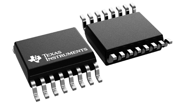
Texas Instruments
ISO1500DBQR
|
Texas Instruments
TLV2372IDG4
|
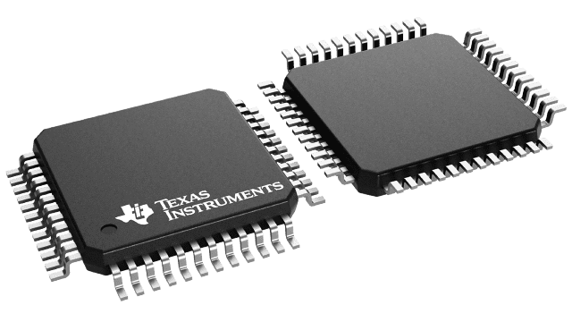
Texas Instruments
DAC5652AIRSLT
|
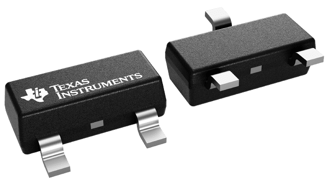
Texas Instruments
DRV5056A1ELPGMQ1
|

Texas Instruments
DRV5056A2EDBZRQ1
|

Texas Instruments
DRV5056A2ELPGMQ1
|

Texas Instruments
DRV5056A4ELPGMQ1
|

Texas Instruments
DRV5056A4ELPGQ1
|
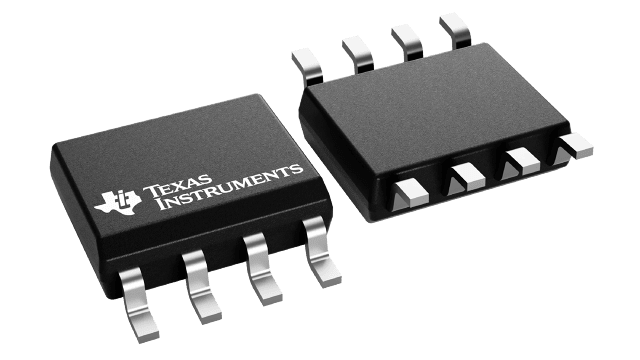
Texas Instruments
OPA2810IDCNR
|
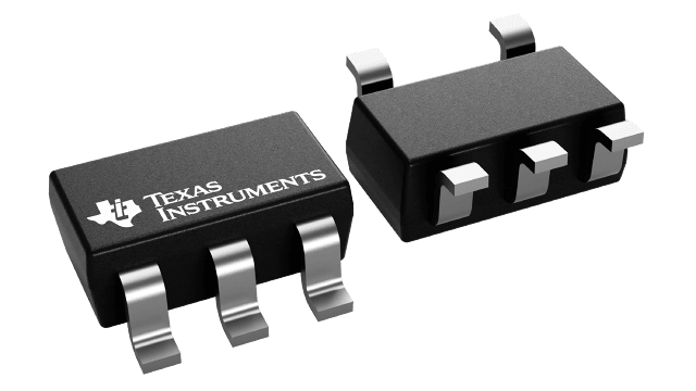
Texas Instruments
SN74LV1T32DCKRG4
|
| Price |
|
|
|
|
|
|
|
|
|
|
|
| RoHS |
|
See ti.com |
Compliant |
Y |
Yes |
Yes |
Yes |
Yes |
Yes |
Compliant |
Compliant |
| Lead Status |
|
See ti.com |
No |
Y |
Yes |
Yes |
Yes |
Yes |
Yes |
No |
No |
| Fail safe |
|
Idle,Open,Short |
|
|
|
|
|
|
|
|
|
| VCC1(Min)(V) |
|
1.71 |
|
|
|
|
|
|
|
|
|
| Rating |
|
Catalog |
|
Catalog |
Automotive |
Automotive |
Automotive |
Automotive |
Automotive |
Catalog |
Catalog |
| Package size |
|
mm2 |
|
mm2 |
mm2 |
mm2 |
mm2 |
mm2 |
mm2 |
mm2 |
mm2 |
| Surge Voltage Capability(Vpk) |
|
4000 |
|
|
|
|
|
|
|
|
|
| Datarate(Mbps) |
|
1 |
|
|
|
|
|
|
|
|
|
| Package Group |
|
SSOP|16 |
|
TQFP|48,VQFN|48 |
SOT-23|3,TO-92|3 |
SOT-23|3,TO-92|3 |
SOT-23|3,TO-92|3 |
SOT-23|3,TO-92|3 |
SOT-23|3,TO-92|3 |
SOIC|8,SOT-23|8,VSSOP|8 |
SC70|5,SOT-23|5 |
| VCC2(Max)(V) |
|
5.5 |
|
|
|
|
|
|
|
|
|
| CSA 61010-1 reinforced working(Vrms) |
|
300 |
|
|
|
|
|
|
|
|
|
| Number of nodes |
|
256 |
|
|
|
|
|
|
|
|
|
| HBM ESD(kV) |
|
16 |
|
|
|
|
|
|
|
|
|
| CSA 60950-1 basic working(Vrms) |
|
370 |
|
|
|
|
|
|
|
|
|
| VCC1(Max)(V) |
|
5.5 |
|
|
|
|
|
|
|
|
|
| CSA isolation rating(Vrms) |
|
3000 |
|
|
|
|
|
|
|
|
|
| DIN V VDE V 0884-10 working voltage(Vpk) |
|
566 |
|
|
|
|
|
|
|
|
|
| Isolation rating(Vrms) |
|
2500 |
|
|
|
|
|
|
|
|
|
| Integrated transformer driver |
|
No |
|
|
|
|
|
|
|
|
|
| Operating temperature range(C) |
|
-40 to 125 |
|
-40 to 85 |
-40 to 150 |
-40 to 150 |
-40 to 150 |
-40 to 150 |
-40 to 150 |
-40 to 125 |
-40 to 125 |
| Approx. price(US$) |
|
2.15 | 1ku |
|
8.15 | 1ku |
0.69 | 1ku |
0.69 | 1ku |
.691 | 1ku |
.691 | 1ku |
.691 | 1ku |
1.70 | 1ku |
0.10 | 1ku |
| VCC2(Min)(V) |
|
4.5 |
|
|
|
|
|
|
|
|
|
| Duplex |
|
Half |
|
|
|
|
|
|
|
|
|
| Resolution(Bits) |
|
|
|
10 |
|
|
|
|
|
|
|
| Features |
|
|
|
Low Power |
|
|
|
|
|
High Cload Drive,Small Size |
|
| SFDR(dB) |
|
|
|
80 |
|
|
|
|
|
|
|
| Interface |
|
|
|
Parallel CMOS |
|
|
|
|
|
|
|
| SNR(dB) |
|
|
|
63 |
|
|
|
|
|
|
|
| Architecture |
|
|
|
Current Source |
|
|
|
|
|
FET,Voltage FB |
|
| Power consumption(Typ)(mW) |
|
|
|
290 |
|
|
|
|
|
|
|
| Accuracy(%) |
|
|
|
|
5 |
5 |
5 |
5 |
5 |
|
|
| Output |
|
|
|
|
0.6 V to Vcc |
0.6 V to Vcc |
0.6 V to Vcc |
0.6 V to Vcc |
0.6 V to Vcc |
|
|
| Supply voltage (Vcc)(Min)(V) |
|
|
|
|
3 |
3 |
3 |
3 |
3 |
|
|
| Bandwidth(kHz) |
|
|
|
|
20 |
20 |
20 |
20 |
20 |
|
|
| Supply voltage (Vcc)(Max)(V) |
|
|
|
|
5.5 |
5.5 |
5.5 |
5.5 |
5.5 |
|
|
| Sensitivity(Typ)(mV/mT) |
|
|
|
|
25,50,100,200 |
25,50,100,200 |
25,50,100,200 |
25,50,100,200 |
25,50,100,200 |
|
|
| Type |
|
|
|
|
Ratiometric Unipolar |
Ratiometric Unipolar |
Ratiometric unipolar |
Ratiometric unipolar |
Ratiometric unipolar |
|
|
| Output current(Typ)(mA) |
|
|
|
|
|
|
|
|
|
75 |
|
| 3rd harmonic(dBc) |
|
|
|
|
|
|
|
|
|
104 |
|
| Offset drift(Typ)(uV/C) |
|
|
|
|
|
|
|
|
|
2 |
|
| BW @ Acl(MHz) |
|
|
|
|
|
|
|
|
|
105 |
|
| Input bias current(Max)(pA) |
|
|
|
|
|
|
|
|
|
20 |
|
| CMRR(Min)(dB) |
|
|
|
|
|
|
|
|
|
90 |
|
| Total Supply Voltage(Max)(+5V=5, +/-5V=10) |
|
|
|
|
|
|
|
|
|
27 |
|
| Vos (offset voltage @ 25 C)(Max)(mV) |
|
|
|
|
|
|
|
|
|
1.5 |
|
| Rail-to-rail |
|
|
|
|
|
|
|
|
|
In,Out |
|
| 2nd harmonic(dBc) |
|
|
|
|
|
|
|
|
|
99 |
|
| @ MHz |
|
|
|
|
|
|
|
|
|
1 |
|
| Acl, min spec gain(V/V) |
|
|
|
|
|
|
|
|
|
1 |
|
| Slew Rate(Typ)(V/us) |
|
|
|
|
|
|
|
|
|
192 |
|
| GBW(Typ)(MHz) |
|
|
|
|
|
|
|
|
|
70 |
|
| CMRR(Typ)(dB) |
|
|
|
|
|
|
|
|
|
100 |
|
| Iq per channel(Typ)(mA) |
|
|
|
|
|
|
|
|
|
3.6 |
|
| Iq per channel(Max)(mA) |
|
|
|
|
|
|
|
|
|
3.8 |
|
| Vn at flatband(Typ)(nV/rtHz) |
|
|
|
|
|
|
|
|
|
6 |
|
| Number of channels(#) |
|
|
|
|
|
|
|
|
|
2 |
|
| Vn at 1 kHz(Typ)(nV/rtHz) |
|
|
|
|
|
|
|
|
|
16.43 |
|
| Total Supply Voltage(Min)(+5V=5, +/-5V=10) |
|
|
|
|
|
|
|
|
|
4.75 |
|
| IOH(Max)(mA) |
|
|
|
|
|
|
|
|
|
|
-8 |
| Logic |
|
|
|
|
|
|
|
|
|
|
True |
| Schmitt Trigger |
|
|
|
|
|
|
|
|
|
|
No |
| ICC @ nom voltage(Max)(mA) |
|
|
|
|
|
|
|
|
|
|
0.01 |
| tpd @ Nom Voltage(Max)(ns) |
|
|
|
|
|
|
|
|
|
|
13,7.5,5.5,7.0 |
| Bits(#) |
|
|
|
|
|
|
|
|
|
|
1 |
| Technology Family |
|
|
|
|
|
|
|
|
|
|
LV1T |
| IOL(Max)(mA) |
|
|
|
|
|
|
|
|
|
|
8 |
| Voltage(Nom)(V) |
|
|
|
|
|
|
|
|
|
|
1.8,2.5,3.3,5.5 |
| VCC(Min)(V) |
|
|
|
|
|
|
|
|
|
|
1.6 |
| VCC(Max)(V) |
|
|
|
|
|
|
|
|
|
|
5.5 |
| F @ nom voltage(Max)(Mhz) |
|
|
|
|
|
|
|
|
|
|
50 |