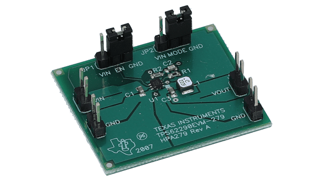
DAC43401DSGRQ1

Texas Instruments DAC43401DSGRQ1

DAC43401DSGTQ1

Texas Instruments DAC43401DSGTQ1

OPA396DCKR

Texas Instruments OPA396DCKR

OPA4191IPWT

Texas Instruments OPA4191IPWT

AMC1202DWVR

Texas Instruments AMC1202DWVR

TLV7044QPWRQ1

Texas Instruments TLV7044QPWRQ1

TPS628680ARQYR

Texas Instruments TPS628680ARQYR

TPS628692ARQYR

Texas Instruments TPS628692ARQYR

LM2902LVQPWRQ1

Texas Instruments LM2902LVQPWRQ1

UCC27614DSGR

Texas Instruments UCC27614DSGR

Price
RoHS Y Y Y Y Y Y Y Y Y Y
Lead Status Y Y Y Y Y Y Y Y Y Y
Architecture String String CMOS CMOS CMOS
Features Small Size,Smart DAC Small Size,Smart DAC e-Trim EMI Hardened,High Cload Drive,Small Size Fail-safe,Hysteresis,POR Adaptive/Dynamic Voltage Scaling,Enable,Forced PWM,I2C/PMBus,Light load efficiency,Output discharge,Over Current Protection,Power good,Soft Start Fixed,Synchronous Rectification,UVLO fixed,VID Interface Adaptive/Dynamic Voltage Scaling,Enable,Forced PWM,I2C/PMBus,Light load efficiency,Output discharge,Over Current Protection,Power good,Soft Start Fixed,Synchronous Rectification,UVLO fixed,VID Interface Cost Optimized,EMI Hardened,Small Size Enable pin,UVLO
INL(max)(n±LSb) 1 1
INL(max)(nLSB) 1 1
Interface type I2C I2C
Number of DAC channels 1 1
Operating temperature range(C) -40 -40 -40 -40 -40 to 125 -40 -40 -40 -40 -40
Output range(max)(mA/V) 5.5 5.5
Output range(min)(mA/V) 1.8 1.8
Output type Buffered Voltage Buffered Voltage Open-collector,Open-drain
Package area(mm^2) 4 4 4.2 32 32 3.75 3.75 32 4
Package size (L x W)(mm) 2 x 2 2 x 2 2 x 2.1 5 x 6.4 5 x 6.4 2.5 x 1.5 2.5 x 1.5 5 x 6.4 2 x 2
Package type WSON WSON SOT-SC70 TSSOP TSSOP VQFN-HR VQFN-HR TSSOP WSON
Pin count 8.0 8.0 5.0 14.0 14.0 9.0 9.0 14.0 8
Power consumption(typ)(mW) 0.18 0.18
Rating Automotive Automotive Catalog Catalog Catalog Automotive Catalog Catalog Automotive Catalog
Reference type Ext,Int Ext,Int
Resolution(Bits) 8 8
Sample/update rate(Msps) 0.022 0.022
Settling time(s) 10 10
TI.com inventory 503901 72878 13588 650 0 121571 93695 27328 105775 310922
Approx. price(US$) .614 | 1ku .718 | 1ku .398 | 1ku 2.66 | 1ku 2.65 | 1ku .655 | 1ku .7 | 1ku .9 | 1ku .081 | 1ku .6 | 1ku
CMRR(typ)(dB) 121 140 92
GBW(typ)(MHz) 1 2.5 1
Input bias current(max)(pA) 10 20 15
Input common mode headroom (to negative supply)(typ)(V) -0.1 -0.1 -0.1
Input common mode headroom (to positive supply)(typ)(V) 0.1 0.1 -1
Iout(typ)(A) 0.06 0.065 0.04
Iq per channel(typ)(mA) 0.0235 0.14 0.000315 0.09
Number of channels 1 4 4 4 1
Offset drift(typ)(V/C) 1 0.1 4
Output swing headroom (to negative supply)(typ)(V) -0.1 0.05 0.04
Output swing headroom (to positive supply)(typ)(V) 0.1 -0.05 -1
Rail-to-rail In,Out In,Out In In to V-
Slew rate(typ)(V/s) 1 5.5 1.5
THD + N at 1 kHz(typ)(%) 0.002 0.0012
TI functional safety category Functional Safety-Capable
TI package name DCK PW PW
Total supply voltage (+5 V = 5, 5 V = 10)(max)(V) 5.5 36 5.5
Total supply voltage (+5 V = 5, 5 V = 10)(min)(V) 1.7 4.5 2.7
Vn at 1 kHz(typ)(nVHz) 60 15 40
Vos (offset voltage at 25C)(max)(mV) 0.1 0.025 8 3
Package Group SOIC|8
Gain error drift (+/-)(Typ)(ppm/C) 3
CMTI(Min)(kV/s) 100
Input range(Vp-p) 0.05
Gain non-linearity (+/-)(Max)(%) 0.03
Isolation working voltage VIOWM (rms)(V) 1000
Isolation transient overvoltage VIOTM (peak)(V) 4250
Gain error (+/-)(Max)(%) 0.2
Small signal bandwidth(Typ)(kHz) 280
Package size mm2
Input offset (+/-)(Max)(mV) 0.05
Input offset drift (+/-)(Typ)(uV/C) 0.15
Input bias current ()(max)(nA) 0.002
Propagation delay time(s) 3 0.017
VICR(max)(V) 6.6
VICR(min)(V) 0
Vs(max)(V) 6.5
Vs(min)(V) 1.6
Control mode DCS-Control DCS-Control
Duty cycle(max)(%) 100 100
Iout(max)(A) 4 6
Iq(typ)(mA) 0.004 0.004
Maximum package height(mm) 1.0 1.0
Regulated outputs(#) 1 1
Switching frequency(max)(kHz) 2400 2400
Switching frequency(min)(kHz) 2400 2400
Type Converter Converter
Vin(max)(V) 5.5 5.5
Vin(min)(V) 2.4 2.4
Vout(max)(V) 0.8375 3.35
Vout(min)(V) 0.2 0.8
DDR memory type LPDDR5
Channel input logic CMOS,TTL
Driver configuration Single
Fall time(ns) 4
Input VCC(max)(V) 26
Input VCC(min)(V) 4.5
Input negative voltage(V) -10
Input threshold CMOS,TTL
Peak output current(A) 10
Power switch IGBT,MOSFET
Rise time(ns) 5
Undervoltage lockout(typ)(V) 4