|
|
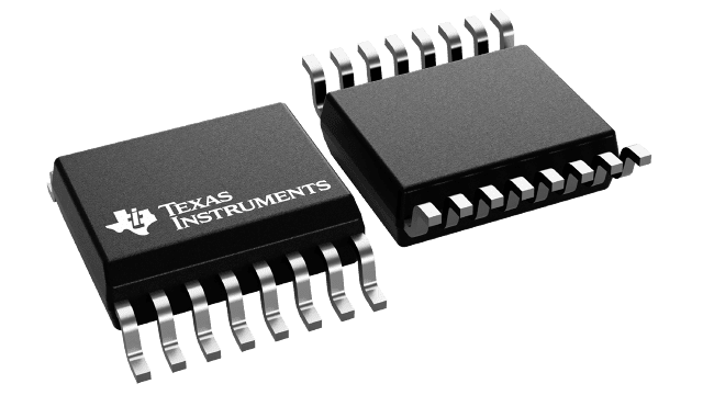
Texas Instruments
ISO7761FDWR
|

Texas Instruments
ADS114S08BIPBSR
|
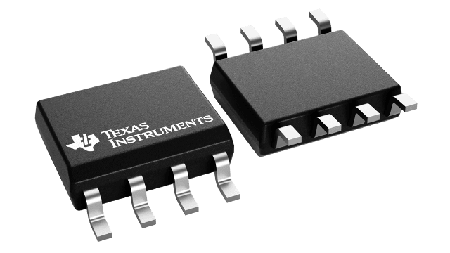
Texas Instruments
THVD1510DR
|

Texas Instruments
ADS114S08BIRHBT
|
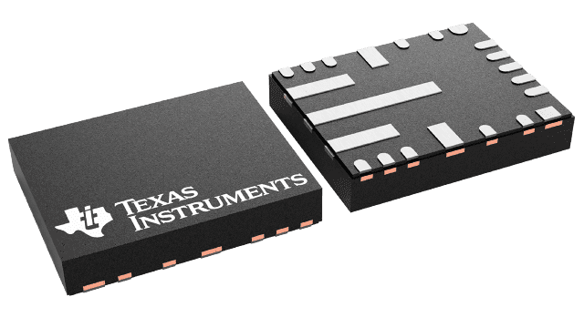
Texas Instruments
LMS3635LQRNLTQ1
|
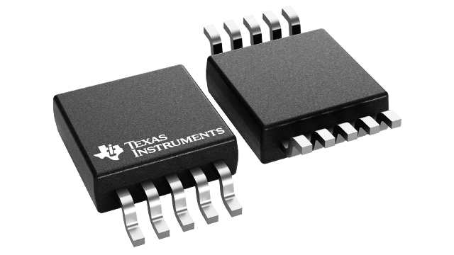
Texas Instruments
THVD1512DGS
|
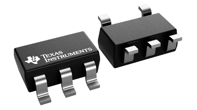
Texas Instruments
TLV70325DBVR
|
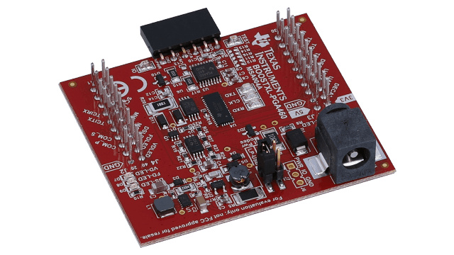
Texas Instruments
BOOSTXL-PGA460
|
Texas Instruments
SN75LVDS82DGGG4
|
Texas Instruments
THS7002IPWPG4
|
| Price |
|
|
|
|
|
|
|
|
|
|
|
| RoHS |
|
Compliant |
Compliant |
Compliant |
Y |
Compliant |
Compliant |
Y |
Not Compliant |
Compliant |
Compliant |
| Lead Status |
|
No |
No |
No |
Y |
No |
No |
Y |
No |
No |
No |
| Forward/reverse channels |
|
5/1 |
|
|
|
|
|
|
|
|
|
| Surge Voltage Capability(Vpk) |
|
12800,6400 |
|
|
|
|
|
|
|
|
|
| Integrated isolated power |
|
No |
|
|
|
|
|
|
|
|
|
| Rating |
|
Catalog |
Catalog |
Catalog |
Catalog |
Automotive |
Catalog |
Catalog |
|
|
|
| Approx. price(US$) |
|
1.78 | 1ku |
|
|
3.95 | 1ku |
|
|
.042 | 1ku |
|
|
|
| Default output |
|
Low |
|
|
|
|
|
|
|
|
|
| Data rate(Max)(Mbps) |
|
100 |
|
|
|
|
|
|
|
|
|
| Isolation rating(Vrms) |
|
5000,3000 |
|
|
|
|
|
|
|
|
|
| Propagation delay(Typ)(ns) |
|
10.7 |
|
|
|
|
|
|
|
|
|
| Propagation delay(ns) |
|
10.7 |
|
|
|
|
|
|
|
|
|
| Package Group |
|
SOIC|16,SSOP|16 |
TQFP,VQFN |
SOIC,VSSOP |
TQFP|32,VQFN|32 |
VQFN-HR |
SOIC,VSSOP |
|
|
|
|
| Operating temperature range(C) |
|
-55 to 125 |
|
|
-40 to 125 |
|
|
-40 |
|
|
|
| Number of channels(#) |
|
6 |
|
|
|
|
|
|
|
|
|
| VCC(Max)(V) |
|
5.5 |
|
|
|
|
|
|
|
|
|
| Package size |
|
mm2 |
|
|
mm2 |
|
|
|
|
|
|
| VCC(Min)(V) |
|
2.25 |
|
|
|
|
|
|
|
|
|
| Digital Supply(Min)(V) |
|
|
2.7 |
|
|
|
|
|
|
|
|
| Package Size |
|
|
mm2 |
|
|
|
|
|
|
|
|
| Features |
|
|
50/60 Hz Rejection,Excitation Current Sources (iDACs),GPIO,Oscillator,PGA,Temp Sensor |
|
50/60 Hz Rejection,Excitation Current Sources (iDACs),GPIO,Oscillator,PGA,Temp Sensor |
Enable,Frequency Synchronization,Light Load Efficiency,Power Good,Pre-Bias Start-Up,Synchronous Rectification |
|
Enable |
|
|
|
| Input Range(Min)(V) |
|
|
0 |
|
|
|
|
|
|
|
|
| Analog Voltage AVDD(Max)(V) |
|
|
5.25 |
|
|
|
|
|
|
|
|
| Interface |
|
|
SPI |
|
SPI |
|
|
|
|
|
|
| INL(Max)(+/-LSB) |
|
|
1 |
|
1 |
|
|
|
|
|
|
| Resolution(Bits) |
|
|
16 |
|
16 |
|
|
|
|
|
|
| Sample Rate(Max)(MSPS) |
|
|
0.004 |
|
|
|
|
|
|
|
|
| Operating Temperature Range(C) |
|
|
-40 to 125 |
-40 to 125 |
|
-40 to 150 |
-40 to 125 |
|
|
|
|
| Sample Rate (max)(SPS) |
|
|
4kSPS |
|
|
|
|
|
|
|
|
| Digital Supply(Max)(V) |
|
|
3.6 |
|
|
|
|
|
|
|
|
| Multi-Channel Configuration |
|
|
Multiplexed |
|
|
|
|
|
|
|
|
| # Input Channels |
|
|
12 |
|
|
|
|
|
|
|
|
| Input Type |
|
|
Differential,Single-Ended |
|
|
|
|
|
|
|
|
| Architecture |
|
|
Delta-Sigma |
|
Delta-Sigma |
|
|
|
|
|
|
| Power Consumption(Typ)(mW) |
|
|
1.75 |
|
|
|
|
|
|
|
|
| Analog Voltage AVDD(Min)(V) |
|
|
2.7 |
|
|
|
|
|
|
|
|
| Input Range(Max)(V) |
|
|
5.25 |
|
|
|
|
|
|
|
|
| Reference Mode |
|
|
Ext,Int |
|
|
|
|
|
|
|
|
| Approx. Price (US$) |
|
|
3.95 | 1ku |
0.79 | 1ku |
|
2.83 | 1ku |
0.95 | 1ku |
|
|
|
|
| Signaling Rate(Max)(Mbps) |
|
|
|
0.5 |
|
|
0.5 |
|
|
|
|
| IEC 61000-4-2 Contact(+/- kV) |
|
|
|
18 |
|
|
18 |
|
|
|
|
| HBM ESD(kV) |
|
|
|
30 |
|
|
30 |
|
|
|
|
| Isolated |
|
|
|
No |
|
|
No |
|
|
|
|
| Supply Voltage(s)(Nom)(V) |
|
|
|
5 |
|
|
5 |
|
|
|
|
| Common Mode Range |
|
|
|
-15 to +15 |
|
|
-15 to |
|
|
|
|
| Fault Protection(V) |
|
|
|
-18 to +18 |
|
|
-18 to |
|
|
|
|
| No. of RX |
|
|
|
1 |
|
|
1 |
|
|
|
|
| Number of Nodes |
|
|
|
256 |
|
|
256 |
|
|
|
|
| No. of TX |
|
|
|
1 |
|
|
1 |
|
|
|
|
| ICC(Max)(mA) |
|
|
|
1 |
|
|
1 |
|
|
|
|
| Duplex |
|
|
|
Half |
|
|
Full |
|
|
|
|
| Power consumption(Typ)(mW) |
|
|
|
|
1.75 |
|
|
|
|
|
|
| Reference mode |
|
|
|
|
Ext,Int |
|
|
|
|
|
|
| Sample rate(Max)(kSPS) |
|
|
|
|
4 |
|
|
|
|
|
|
| Input range(Min)(V) |
|
|
|
|
-2.625,0 |
|
|
|
|
|
|
| Multi-channel configuration |
|
|
|
|
Multiplexed |
|
|
|
|
|
|
| Analog voltage AVDD(Min)(V) |
|
|
|
|
2.7 |
|
|
|
|
|
|
| Number of input channels |
|
|
|
|
12 |
|
|
|
|
|
|
| Digital supply(Max)(V) |
|
|
|
|
3.6 |
|
|
|
|
|
|
| Digital supply(Min)(V) |
|
|
|
|
2.7 |
|
|
|
|
|
|
| Input range(Max)(V) |
|
|
|
|
2.625,5.25 |
|
|
|
|
|
|
| Input type |
|
|
|
|
Differential,Single-Ended |
|
|
|
|
|
|
| Analog voltage AVDD(Max)(V) |
|
|
|
|
5.25 |
|
|
|
|
|
|
| Switching Frequency(Min)(kHz) |
|
|
|
|
|
250 |
|
|
|
|
|
| Control Mode |
|
|
|
|
|
Current Mode |
|
|
|
|
|
| Switching Frequency(Max)(kHz) |
|
|
|
|
|
500 |
|
|
|
|
|
| Duty Cycle(Max)(%) |
|
|
|
|
|
98 |
|
|
|
|
|
| Type |
|
|
|
|
|
Converter |
|
|
|
|
|
| Regulated Outputs(#) |
|
|
|
|
|
1 |
|
|
|
|
|
| Vout(Max)(V) |
|
|
|
|
|
15 |
|
|
|
|
|
| Vin(Max)(V) |
|
|
|
|
|
42 |
|
|
|
|
|
| Iq(Typ)(mA) |
|
|
|
|
|
0.015 |
|
|
|
|
|
| Vout(Min)(V) |
|
|
|
|
|
1 |
|
|
|
|
|
| Vin(Min)(V) |
|
|
|
|
|
3.5 |
|
|
|
|
|
| Iout(Max)(A) |
|
|
|
|
|
3.5 |
|
|
|
|
|
| Accuracy(%) |
|
|
|
|
|
|
|
2 |
|
|
|
| Dropout voltage (Vdo)(typ)(mV) |
|
|
|
|
|
|
|
220 |
|
|
|
| Fixed output options(V) |
|
|
|
|
|
|
|
2.5 |
|
|
|
| Iout(max)(A) |
|
|
|
|
|
|
|
0.3 |
|
|
|
| Iq(typ)(mA) |
|
|
|
|
|
|
|
0.035 |
|
|
|
| Load capacitance(min)(F) |
|
|
|
|
|
|
|
0.1 |
|
|
|
| Maximum package height(mm) |
|
|
|
|
|
|
|
1.45 |
|
|
|
| Noise(Vrms) |
|
|
|
|
|
|
|
48 |
|
|
|
| Output options |
|
|
|
|
|
|
|
Fixed Output |
|
|
|
| PSRR at 100 KHz(dB) |
|
|
|
|
|
|
|
52 |
|
|
|
| Package area(mm^2) |
|
|
|
|
|
|
|
8.12 |
|
|
|
| Package size (L x W)(mm) |
|
|
|
|
|
|
|
2.9 x 2.8 |
|
|
|
| Package type |
|
|
|
|
|
|
|
SOT-23 |
|
|
|
| Pin count |
|
|
|
|
|
|
|
5.0 |
|
|
|
| Regulated outputs(#) |
|
|
|
|
|
|
|
1 |
|
|
|
| TI functional safety category |
|
|
|
|
|
|
|
|
|
|
|
| Thermal resistance JA(C/W) |
|
|
|
|
|
|
|
254.1 |
|
|
|
| Vin(max)(V) |
|
|
|
|
|
|
|
5.5 |
|
|
|
| Vin(min)(V) |
|
|
|
|
|
|
|
2 |
|
|
|
| Vout(max)(V) |
|
|
|
|
|
|
|
3.3 |
|
|
|
| Vout(min)(V) |
|
|
|
|
|
|
|
1 |
|
|
|
| TI.com inventory |
|
|
|
|
|
|
|
296632 |
|
|
|