|
|
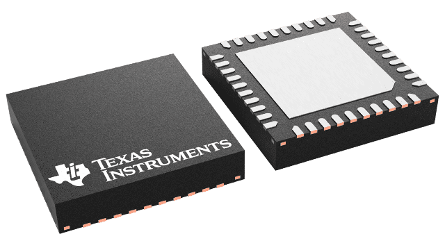
Texas Instruments
LP5860RKPR
|
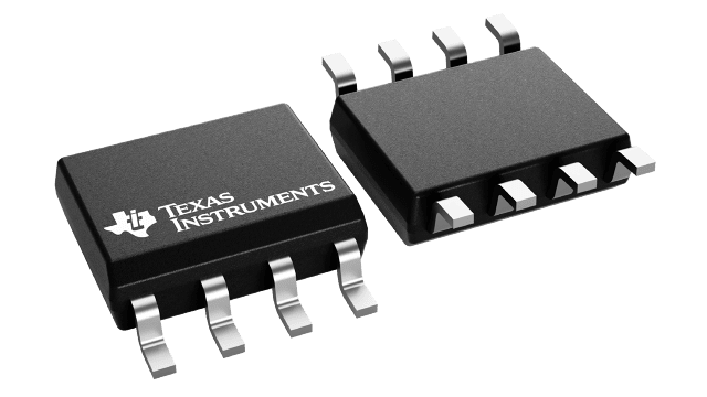
Texas Instruments
TCAN1044ADDFRQ1
|
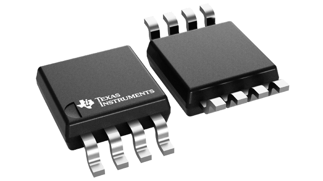
Texas Instruments
TMAG5170A2EDGKRQ1
|
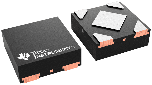
Texas Instruments
TPS7A03175PYCHR
|
Texas Instruments
TRSF3243EIRHBR
|
Texas Instruments
TPS53689TRSBR
|
Texas Instruments
INA241A2QDGKRQ1
|
Texas Instruments
INA241B3QDGKRQ1
|
Texas Instruments
INA296A1QDGKRQ1
|
Texas Instruments
INA296A3QDGKRQ1
|
| Price |
|
|
|
|
|
|
|
|
|
|
|
| RoHS |
|
Y |
Y |
Y |
Y |
Y |
Y |
Y |
Y |
Y |
Y |
| Lead Status |
|
Y |
Y |
Y |
Y |
Y |
Y |
Y |
Y |
Y |
Y |
| Features |
|
Analog/PWM mixed dimming,Constant current,Enable/Shutdown,LED Open Detection,LED Short Detection,SPI/I2C,Thermal shutdown |
|
|
Enable,Output discharge |
Auto-Powerdown |
Adjustable current limit,Dynamic Voltage Scaling,Enable,Frequency synchronization,I2C,Light Load Efficiency,Multiple Outputs,PMBus,Phase Interleaving,Power good,Pre-Bias Start-Up,Remote Sense,SVID,Synchronous Rectification,UVLO adjustable,Voltage Margining |
Bi-directional,Bidirectional,Enhanced PWM Rejection,Low-side Capable,Ultra precise |
Bi-directional,Bidirectional,Enhanced PWM Rejection,High precision,Low-side Capable |
Bi-directional,Bidirectional,Low-side Capable,Ultra precise |
Bi-directional,Bidirectional,Low-side Capable,Ultra precise |
| Iout(max)(A) |
|
0.9 |
|
|
0.2 |
|
765 |
|
|
|
|
| Iq(typ)(mA) |
|
4.3 |
|
|
0.0002 |
|
50 |
|
|
|
|
| LED configuration |
|
Matrix |
|
|
|
|
|
|
|
|
|
| LED current per channel(mA) |
|
50 |
|
|
|
|
|
|
|
|
|
| Number of channels |
|
18 |
|
|
|
|
|
1 |
1 |
1 |
1 |
| Operating temperature range(C) |
|
-40 |
-40 to 150 |
-40 |
-40 |
-40 |
-40 |
-40 |
-40 |
-40 |
-40 |
| Package area(mm^2) |
|
25 |
|
14.7 |
0.405769 |
25 |
25 |
|
|
|
|
| Package size (L x W)(mm) |
|
5 x 5 |
|
3 x 4.9 |
0.637 x 0.637 |
5 x 5 |
5 x 5 |
3 x 4.9 |
3 x 4.9 |
3 x 4.9 |
3 x 4.9 |
| Package type |
|
VQFN |
|
VSSOP |
DSBGA |
VQFN |
WQFN |
VSSOP |
VSSOP |
VSSOP |
VSSOP |
| Pin count |
|
40 |
|
8 |
4 |
32 |
40 |
|
|
|
|
| Program memory |
|
Yes |
|
|
|
|
|
|
|
|
|
| Rating |
|
Catalog |
Automotive |
Catalog |
Catalog |
Catalog |
Catalog |
Automotive |
Automotive |
Automotive |
Automotive |
| Shutdown current (ISD)(typ)(A) |
|
1 |
|
|
|
|
|
|
|
|
|
| Topology |
|
Linear |
|
|
|
|
|
|
|
|
|
| Vin(max)(V) |
|
5.5 |
|
|
6 |
|
17 |
|
|
|
|
| Vin(min)(V) |
|
2.7 |
|
|
1.5 |
|
4.5 |
|
|
|
|
| TI.com inventory |
|
109 |
0 |
6981 |
179500 |
66184 |
760 |
3144 |
2908 |
3294 |
3131 |
| Approx. price(US$) |
|
.813 | 1ku |
.319 | 1ku |
.91 | 1ku |
.113 | 1ku |
1.07 | 1ku |
3.05 | 1ku |
1.593 | 1ku |
1.121 | 1ku |
1.593 | 1ku |
1.593 | 1ku |
| Package Group |
|
|
SOIC|8,SON|8,SOT-23-THIN|8 |
|
|
|
|
|
|
|
|
| Protocols |
|
|
CAN,CAN FD |
|
|
|
|
|
|
|
|
| Common mode voltage(V) |
|
|
-12 to 12 |
|
|
|
|
|
|
|
|
| TI functional safety category |
|
|
Functional Safety-Capable |
Functional Safety-Compliant |
|
|
|
|
|
|
|
| Number of channels(#) |
|
|
1 |
|
|
|
|
|
|
|
|
| Package size |
|
|
mm2 |
|
|
|
|
|
|
|
|
| Supply voltage(V) |
|
|
4.5 to 5.5 |
|
|
|
|
|
|
|
|
| Isolated |
|
|
No |
|
|
|
|
|
|
|
|
| Signaling rate(Max)(Mbps) |
|
|
8 |
|
|
|
|
|
|
|
|
| Low power mode |
|
|
Standby |
|
|
|
|
|
|
|
|
| Bus fault voltage(V) |
|
|
-58 to 58 |
|
|
|
|
|
|
|
|
| Interface type |
|
|
|
SPI |
|
|
|
|
|
|
|
| Magnetic sensing range(mT) |
|
|
|
150,300,75 |
|
|
|
|
|
|
|
| Pitch(mm) |
|
|
|
0.65 |
|
|
|
|
|
|
|
| Sample rate(ksps) |
|
|
|
20 |
|
|
|
|
|
|
|
| Sensitivity error(%) |
|
|
|
2.5 |
|
|
|
|
|
|
|
| Supply voltage(max)(V) |
|
|
|
5.5 |
|
|
|
20 |
20 |
20 |
20 |
| Supply voltage(min)(V) |
|
|
|
2.3 |
|
|
|
2.7 |
2.7 |
2.7 |
2.7 |
| Type |
|
|
|
3-Axis linear |
|
|
Controller |
|
|
|
|
| Accuracy(%) |
|
|
|
|
1.5 |
|
|
|
|
|
|
| Dropout voltage (Vdo)(typ)(mV) |
|
|
|
|
205 |
|
|
|
|
|
|
| Fixed output options(V) |
|
|
|
|
1.75 |
|
|
|
|
|
|
| Load capacitance(min)(F) |
|
|
|
|
1 |
|
|
|
|
|
|
| Maximum package height(mm) |
|
|
|
|
0.4 |
|
0.8 |
|
|
|
|
| Noise(Vrms) |
|
|
|
|
130 |
|
|
|
|
|
|
| Output options |
|
|
|
|
Fixed Output |
|
|
|
|
|
|
| PSRR at 100 KHz(dB) |
|
|
|
|
35 |
|
|
|
|
|
|
| Regulated outputs(#) |
|
|
|
|
1 |
|
2 |
|
|
|
|
| Thermal resistance JA(C/W) |
|
|
|
|
201.1 |
|
|
|
|
|
|
| Vout(max)(V) |
|
|
|
|
5 |
|
5.5 |
|
|
|
|
| Vout(min)(V) |
|
|
|
|
0.8 |
|
0.25 |
|
|
|
|
| Data rate(max)(MBits) |
|
|
|
|
|
1 |
|
|
|
|
|
| Data rate(max)(Mbps) |
|
|
|
|
|
1 |
|
|
|
|
|
| Drivers per package |
|
|
|
|
|
3 |
|
|
|
|
|
| ESD HBM(kV) |
|
|
|
|
|
15 |
|
|
|
|
|
| Logic voltage(min)(V) |
|
|
|
|
|
3.3 |
|
|
|
|
|
| Main supply voltage(nom)(V) |
|
|
|
|
|
3.3, 5 |
|
|
|
|
|
| Receivers per package |
|
|
|
|
|
5 |
|
|
|
|
|
| Vout(typ)(V) |
|
|
|
|
|
5.4 |
|
|
|
|
|
| Control mode |
|
|
|
|
|
|
D-CAP+ |
|
|
|
|
| Number of phases |
|
|
|
|
|
|
8 |
|
|
|
|
| Switching frequency(max)(kHz) |
|
|
|
|
|
|
1500 |
|
|
|
|
| Switching frequency(min)(kHz) |
|
|
|
|
|
|
300 |
|
|
|
|
| Bandwidth(kHz) |
|
|
|
|
|
|
|
1100 |
1000,1100 |
1000,1100 |
1000,1100 |
| CMRR(min)(dB) |
|
|
|
|
|
|
|
150 |
120 |
150 |
150 |
| Common-mode voltage(max)(V) |
|
|
|
|
|
|
|
110 |
110 |
110 |
110 |
| Common-mode voltage(min)(V) |
|
|
|
|
|
|
|
-5 |
-5 |
-5 |
-5 |
| Comparators(#) |
|
|
|
|
|
|
|
0 |
0 |
0 |
0 |
| Gain error drift ()(max)(ppm/C) |
|
|
|
|
|
|
|
1 |
5 |
1 |
1 |
| Gain error(%) |
|
|
|
|
|
|
|
0.01,0.015 |
0.1 |
0.01,0.015 |
0.01,0.015 |
| Input offset ()(max)(V) |
|
|
|
|
|
|
|
10,15,20,8 |
150 |
10,15,20,8 |
10,15,20,8 |
| Input offset drift ()(typ)(V/C) |
|
|
|
|
|
|
|
0.05,0.1 |
0.5 |
0.1 |
0.1 |
| Iq(max)(mA) |
|
|
|
|
|
|
|
3.2 |
3.2 |
3.2 |
3.2 |
| Product type |
|
|
|
|
|
|
|
Analog output |
Analog output |
Analog output |
Analog output |
| Slew rate(V/s) |
|
|
|
|
|
|
|
5 |
5 |
8 |
8 |
| Voltage gain(V/V) |
|
|
|
|
|
|
|
10,100,20,200,50 |
10,100,20,200,50,500 |
10,100,20,200,50 |
10,100,20,200,50 |