LT3582EUD Demo Board | 2.7V-5.5VIN, Programmable Vout Boost and Inverting DC/DC Converters with OTP (Requires DC590)
Analog Devices Inc.
Demonstration circuit 1247A features the LT3582 an I2C Programmable Boost and Single Inductor Inverting DC/DC Converters with OTP. It converts a 2.7V-5.5V source to two outputs, a positive and a negative. The positive output can be programmed from 3.2V to 12.775V at 25mV intervals and the negative from -1.2V to -13.95V at 50mV intervals, all via the QuickEval™ System. A DC590B is needed for evaluation of this demo board. Table 1 below shows the maximum expected load currents for some output/input combinations. Check Maximum Load Current section on datasheet for other combinations. The LT3582 features all integrated switches and feedback resistors, a low noise control scheme, positive output disconnect function, low quiescent current, built in softstart.
| Distributor | SKU | Stock | MOQ | 1 | 10 | 50 | 100 | 1,000 | 10,000 |
|---|---|---|---|---|---|---|---|---|---|
| DigiKey | 505-DC1247A-ND | 2 | 1 | $172.06 | $172.06 | $172.06 | $172.06 | $172.06 | $172.06 |
| Analog Devices Inc | DC1247A | 0 | $147.12 | $147.12 | $147.12 | $147.12 | $147.12 | $147.12 | |
| Arrow North American Components | DC1247A | 0 | 1 | $145.31 | $143.86 | $140.99 | $139.58 | $135.44 | $134.08 |
| element14 APAC | DC1247A | 5 | 1 | * $187.55 | * $187.55 | * $187.55 | * $187.55 | * $187.55 | * $187.55 |
| Farnell | DC1247A | 5 | 1 | * $171.49 | * $171.49 | * $171.49 | * $171.49 | * $171.49 | * $171.49 |
| Mouser Electronics | 584-DC1247A | 3 | 1 | $153.03 | $153.03 | $153.03 | $153.03 | $153.03 | $153.03 |
| Newark | DC1247A | 5 | 1 | $152.81 | $152.81 | $152.81 | $152.81 | $152.81 | $152.81 |
| Verical Marketplace | DC1247A | 5 | 1 | $145.58 | $145.58 | $145.58 | $145.58 | $145.58 | $145.58 |
LTC3775EUD Demo Board | 5V ≤ VIN ≤ 26V, VOUT = 1.2V @ 15A
Analog Devices Inc.
Demonstration circuit 1290A is a high frequency synchronous step-down converter featuring the LTC3775EUD. The package style for the LTC3775EUD is a 16-pin 3mm x 3mm QFN. Two versions of the demonstration board are available. DC-1290A-A has been optimized for 5V to 26V input and typically provides 1.2V/15A, while the DC1290A-B is optimized for 5V to 36VIN range and typically provides 1.2V/10A.
| Distributor | SKU | Stock | MOQ | 1 | 10 | 50 | 100 | 1,000 | 10,000 |
|---|---|---|---|---|---|---|---|---|---|
| DigiKey | DC1290A-A-ND | 0 | 1 | $138.47 | $138.47 | $138.47 | $138.47 | $138.47 | $138.47 |
| Analog Devices Inc | DC1290A-A | 0 | $117.70 | $117.70 | $117.70 | $117.70 | $117.70 | $117.70 | |
| Arrow North American Components | DC1290A-A | 0 | 1 | $116.25 | $115.08 | $112.79 | $111.67 | $108.35 | $107.27 |
| Mouser Electronics | 584-DC1290A-A | 5 | 1 | $122.42 | $122.42 | $122.42 | $122.42 | $122.42 | $122.42 |
| Verical Marketplace | DC1290A-A | 1 | 1 | $116.46 | $116.46 | $116.46 | $116.46 | $116.46 | $116.46 |
DC1323A
Analog Devices Inc.
The LT3686 is a current mode PWM step-down DC/DC converter with an internal 1.2A power switch, packaged in 10-lead 3mm ? 3mm DFN. The wide input range of 3.6V to 37V makes the LT3686 suitable for regulating power from a wide variety of sources, including 24V industrial supplies and automotive batteries. Its high maximum frequency allows the use of tiny inductors and capacitors, resulting in a very small solution. Operating frequency above the AM band avoids interfering with radio reception, making the LT3686 particularly suitable for automotive applications.Cycle-by-cycle current limit and DA current sense provide protection against fault conditions. Soft-start and frequency foldback eliminate input current surge during start-up. An optional internal regulated active load at the output via the BD pin keeps the LT3686 at full switching frequency at light loads, resulting in low, predictable output ripple above the audio and AM bands. Internal compensation and an internal boost diode reduce external component count. Overvoltage Protections Features LT3686 55V - LT3686A 60V External Synchronization Applications Automotive Systems Battery-Powered Equipment Wall Transformer Regulation Distributed Supply Regulation
| Distributor | SKU | Stock | MOQ | 1 | 10 | 50 | 100 | 1,000 | 10,000 |
|---|---|---|---|---|---|---|---|---|---|
| DigiKey | 505-DC1323A-ND | 1 | 1 | $138.47 | $138.47 | $138.47 | $138.47 | $138.47 | $138.47 |
| Analog Devices Inc | DC1323A | 0 | $147.12 | $147.12 | $147.12 | $147.12 | $147.12 | $147.12 | |
| Arrow North American Components | DC1323A | 0 | 1 | $139.84 | $138.44 | $135.69 | $134.33 | $130.34 | $129.04 |
| Mouser Electronics | 584-DC1323A | 0 | 1 | $152.26 | $152.26 | $152.26 | $152.26 | $152.26 | $152.26 |
DC1329A
Analog Devices Inc.
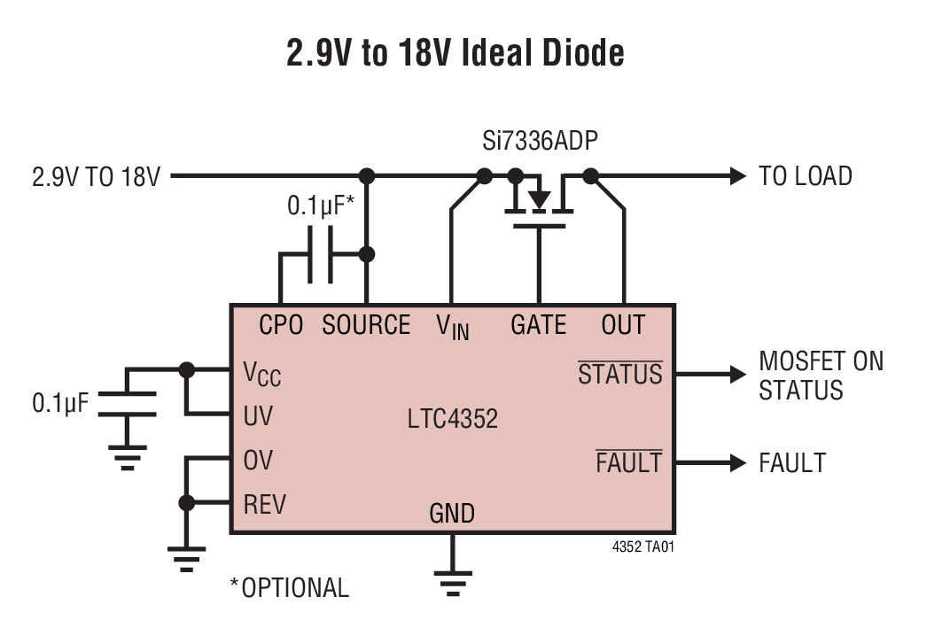
The LTC4352 creates a near-ideal diode using an external N-channel MOSFET. It replaces a high power Schottky diode and the associated heat sink, saving power and board area. The ideal diode function permits low loss power ORing and supply holdup applications. The LTC4352 regulates the forward voltage drop across the MOSFET to ensure smooth current transfer in diode-OR applications. A fast turn-on reduces the load voltage droop during supply switch-over. If the input supply fails or is shorted, a fast turn-off minimizes reverse currents. The controller operates with supplies from 2.9V to 18V. For lower voltages, an external supply is needed at the VCC pin. Power passage is disabled during undervoltage or overvoltage conditions. The controller also features an open MOSFET detect circuit that ?ags excessive voltage drop across the pass transistor in the on state. A REV pin enables reverse current, overriding the diode behavior when desired.Applications Redundant Power Supplies Supply Holdup Telecom Infrastructure Computer Systems and Servers
| Distributor | SKU | Stock | MOQ | 1 | 10 | 50 | 100 | 1,000 | 10,000 |
|---|---|---|---|---|---|---|---|---|---|
| DigiKey | DC1329A-ND | 1 | 1 | $70.52 | $70.52 | $70.52 | $70.52 | $70.52 | $70.52 |
| Analog Devices Inc | DC1329A | 0 | $58.85 | $58.85 | $58.85 | $58.85 | $58.85 | $58.85 | |
| Arrow North American Components | DC1329A | 0 | 1 | $55.49 | $55.49 | $55.49 | $55.49 | $55.49 | $55.49 |
| element14 APAC | DC1329A | 10 | 1 | * $76.78 | * $76.78 | * $76.78 | * $76.78 | * $76.78 | * $76.78 |
| Farnell | DC1329A | 10 | 1 | * $70.28 | * $70.28 | * $70.28 | * $70.28 | * $70.28 | * $70.28 |
| Mouser Electronics | 584-DC1329A | 4 | 1 | $60.89 | $60.89 | $60.89 | $60.89 | $60.89 | $60.89 |
| Newark | DC1329A | 10 | 1 | $62.63 | $62.63 | $62.63 | $62.63 | $62.63 | $62.63 |
| Verical Marketplace | DC1329A | 14 | 1 | $58.23 | $58.23 | $58.23 | $58.23 | $58.23 | $58.23 |
LT1575 | Ultra Fast Transient Response Linear Regulator
Analog Devices Inc.
The LT1575/LT1577 are single/dual controller ICs that drive low cost external N-channel MOSFETs as source followers to produce ultrafast transient response, low dropout voltage regulators.The LT1575/LT1577 achieve unprecedented transient-load performance by eliminating expensive tantalum or bulk electrolytic output capacitors in the most demanding modern microprocessor applications. Precision-trimmed adjustable and fixed output voltage versions accommodate any required microprocessor power supply voltage. Selection of the N-channel MOSFET RDS(ON) allows very low dropout voltages to be achieved.Unique protection features include a high side current limit amplifier that activates a fault protection timer circuit. A multifunction Shutdown pin provides either current limit time-out with latch off, overvoltage protection, thermal shutdown or a combination of these functions. The LT1575 is available in 8-pin SO or PDIP and the LT1577 is available in 16-pin narrow body SO.Applications Pentium? Processor Supplies PowerPC? Supplies 5V to 3.XXV or 3.3V to 2.XXV Microprocessor Supplies GTL Termination Low Voltage Logic Supplies
| Distributor | SKU | Stock | MOQ | 1 | 10 | 50 | 100 | 1,000 | 10,000 |
|---|---|---|---|---|---|---|---|---|---|
| DigiKey | 505-DC136A-ND | 16 | 1 | $62.71 | $62.71 | $62.71 | $62.71 | $62.71 | $62.71 |
| Arrow North American Components | DC136A | 1 | 1 | $62.00 | $57.86 | $56.71 | $56.14 | $54.47 | $53.93 |
| Mouser Electronics | N/A | 0 | |||||||
| Verical Marketplace | DC136A | 1 | 1 | $62.00 | $62.00 | $62.00 | $62.00 | $62.00 | $62.00 |
DC1370A-I
Analog Devices Inc.
The LTC2261-12/LTC2260-12/LTC2259-12 are sampling 12-bit A/D converters designed for digitizing high frequency, wide dynamic range signals. They are perfect for demanding communications applications with AC performance that includes 70.8dB SNR and 85dB spurious free dynamic range (SFDR). Ultralow jitter of 0.17psRMS allows undersampling of IF frequencies with excellent noise performance.DC specs include ?0.3LSB INL (typical), ?0.1LSB DNL (typical) and no missing codes over temperature. The transition noise is a low 0.3LSBRMS.The digital outputs can be either full-rate CMOS, double-data rate CMOS, or double-data rate LVDS. A separate output power supply allows the CMOS output swing to range from 1.2V to 1.8V.The ENC+ and ENC? inputs may be driven differentially or single ended with a sine wave, PECL, LVDS, TTL or CMOS inputs. An optional clock duty cycle stabilizer allows high performance at full speed for a wide range of clock duty cycles. Bits LTC2259-12 12 LTC2259-14 14 LTC2259-16 14 Applications Communications Cellular Base Stations Software Defined Radios Portable Medical Imaging Multi-Channel Data Acquisition Nondestructive Testing
| Distributor | SKU | Stock | MOQ | 1 | 10 | 50 | 100 | 1,000 | 10,000 |
|---|---|---|---|---|---|---|---|---|---|
| DigiKey | DC1370A-I-ND | 2 | $252.13 | $252.13 | $252.13 | $252.13 | $252.13 | $252.13 | |
| Analog Devices Inc | DC1370A-I | 0 | $256.80 | $256.80 | $256.80 | $256.80 | $256.80 | $256.80 | |
| Arrow North American Components | DC1370A-I | 0 | 1 | $208.70 | $208.70 | $208.70 | $208.70 | $208.70 | $208.70 |
| Mouser Electronics | 584-DC1370A-I | 0 | 1 | $267.09 | $267.09 | $267.09 | $267.09 | $267.09 | $267.09 |
| Verical Marketplace | DC1370A-I | 6 | 1 | $228.57 | $219.18 | $219.18 | $219.18 | $219.18 | $219.18 |
LTC2262-12 | 12-bit, 150Msps ADC, CMOS Outputs, 5-170MHz, Requires DC890 and DC1075
Analog Devices Inc.
DC1370A-N: Demo Board for the LTC2262-12 12-Bit, 150Msps Ultralow Power 1.8V ADC
| Distributor | SKU | Stock | MOQ | 1 | 10 | 50 | 100 | 1,000 | 10,000 |
|---|---|---|---|---|---|---|---|---|---|
| DigiKey | DC1370A-N-ND | 0 | 1 | $271.86 | $271.86 | $271.86 | $271.86 | $271.86 | $271.86 |
| Analog Devices Inc | DC1370A-N | 0 | $235.40 | $235.40 | $235.40 | $235.40 | $235.40 | $235.40 | |
| Arrow North American Components | DC1370A-N | 0 | 1 | $232.49 | $230.17 | $225.59 | $223.33 | $216.70 | $214.53 |
| Mouser Electronics | 584-DC1370A-N | 0 | 1 | $244.83 | $244.83 | $244.83 | $244.83 | $244.83 | $244.83 |
| Verical Marketplace | DC1370A-N | 13 | 1 | $251.43 | $237.84 | $237.84 | $237.84 | $237.84 | $237.84 |
EVAL-AD7718EBZ
Analog Devices Inc.
The AD7708/18 are complete analog front-ends for low frequency measurement applications. The AD7718 contains a 24-bit sigma delta ADC with PGA and can be configured as 4/5 fully-differential input channels or 8/10 pseudo-differential input channels. Two pins on the device are configurable as analog inputs or reference inputs. The AD7708 is a 16-bit version of the AD7718. Inputs signal ranges from 20mV to 2.56V can be directly converted using these ADCs. Signals can be converted directly from a transducer without the need for signal conditioning.
| Distributor | SKU | Stock | MOQ | 1 | 10 | 50 | 100 | 1,000 | 10,000 |
|---|---|---|---|---|---|---|---|---|---|
| DigiKey | EVAL-AD7718EBZ-ND | 0 | 1 | $85.27 | $85.27 | $85.27 | $85.27 | $85.27 | $85.27 |
| Analog Devices Inc | EVAL-AD7718EBZ | 0 | $67.06 | $67.06 | $67.06 | $67.06 | $67.06 | $67.06 | |
| Arrow North American Components | EVAL-AD7718EBZ | 0 | 1 | $70.36 | $69.66 | $68.27 | $67.59 | $65.58 | $64.92 |
| element14 APAC | EVAL-AD7718EBZ | 0 | 1 | * $70.86 | * $70.86 | * $70.86 | * $70.86 | * $70.86 | * $70.86 |
| Farnell | EVAL-AD7718EBZ | 0 | 1 | * $59.41 | * $59.41 | * $59.41 | * $59.41 | * $59.41 | * $59.41 |
| Mouser Electronics | 584-EVAL-AD7718EBZ | 2 | 1 | $69.75 | $69.75 | $69.75 | $69.75 | $69.75 | $69.75 |
| Verical Marketplace | EVAL-AD7718EBZ | 8 | 1 | $66.36 | $63.31 | $62.44 | $62.44 | $62.44 | $62.44 |
| Distributor | SKU | Stock | MOQ | 1 | 10 | 50 | 100 | 1,000 | 10,000 |
|---|---|---|---|---|---|---|---|---|---|
| DigiKey | 1127-1868-1-ND | 24 | 1 | $23.62 | $18.95 | $17.78 | $17.32 | $15.52 | $15.52 |
| Arrow North American Components | HMC788ALP2E | 2 | 1 | $16.28 | $20.96 | $20.96 | $20.96 | $20.96 | $20.96 |
| element14 APAC | HMC788ALP2E | 46 | 1 | * $23.22 | * $20.25 | * $19.22 | * $17.80 | * $16.95 | * $16.95 |
| Farnell | HMC788ALP2E | 46 | 1 | * $22.52 | * $19.63 | * $18.62 | * $17.25 | * $16.35 | * $16.35 |
| Mouser Electronics | 584-HMC788ALP2E | 930 | 1 | $23.38 | $18.81 | $17.56 | $15.78 | $14.42 | $14.13 |
| Newark | HMC788ALP2E | 49 | 1 | $20.44 | $17.82 | $16.29 | $15.66 | $15.66 | $15.66 |
| Win Source | HMC788ALP2E | 11434 | 6 | $12.01 | $9.94 | $9.94 | $9.94 | $9.94 |
| Distributor | SKU | Stock | MOQ | 1 | 10 | 50 | 100 | 1,000 | 10,000 |
|---|---|---|---|---|---|---|---|---|---|
| DigiKey | 505-HMC832ALP6GETR-ND | 0 | $20.89 | $19.82 | $19.00 | $16.74 | $15.99 | $15.99 | |
| Arrow North American Components | HMC832ALP6GE | 49 | 51 | $0.00 | $0.00 | $0.00 | $9.69 | $9.13 | $8.86 |
| Mouser Electronics | 584-HMC832ALP6GE | 0 | 1 | $20.34 | |||||
| Newark | HMC832ALP6GE | 0 | $22.97 | $22.97 | $20.84 | $19.09 | $16.57 | $16.57 | |
| Verical Marketplace | HMC832ALP6GE | 450 | 1 | $20.87 | $18.30 | $0.00 | $15.71 | $13.66 | $13.66 |


