
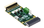
EVAL-SSM2377Z
Analog Devices Inc.
| Distributor | SKU | Stock | MOQ | 1 | 10 | 50 | 100 | 1,000 | 10,000 |
|---|---|---|---|---|---|---|---|---|---|
| DigiKey | EVAL-SSM2377Z-ND | 0 | 1 | $91.66 | $91.66 | $91.66 | $91.66 | $91.66 | $91.66 |
| Analog Devices Inc | EVAL-SSM2377Z | 0 | $83.78 | $83.78 | $83.78 | $83.78 | $83.78 | $83.78 | |
| Arrow North American Components | EVAL-SSM2377Z | 0 | 1 | $86.32 | $85.45 | $83.75 | $82.92 | $80.45 | $79.65 |
| element14 APAC | EVAL-SSM2377Z | 0 | 1 | * $78.23 | * $78.23 | * $78.23 | * $78.23 | * $78.23 | * $78.23 |
| Farnell | EVAL-SSM2377Z | 0 | 1 | * $66.44 | * $66.44 | * $66.44 | * $66.44 | * $66.44 | * $66.44 |
| Mouser Electronics | 584-EVAL-SSM2377Z | 1 | 1 | $68.16 | $68.16 | $68.16 | $68.16 | $68.16 | $68.16 |
| Newark | EVAL-SSM2377Z | 0 | $65.25 | $65.25 | $65.25 | $65.25 | $65.25 | $65.25 | |
| Verical Marketplace | EVAL-SSM2377Z | 19 | 1 | $82.89 | $82.89 | $82.89 | $82.89 | $82.89 | $82.89 |

EVAL-SSM3515Z
Analog Devices Inc.
| Distributor | SKU | Stock | MOQ | 1 | 10 | 50 | 100 | 1,000 | 10,000 |
|---|---|---|---|---|---|---|---|---|---|
| DigiKey | 505-EVAL-SSM3515Z-ND | 0 | 1 | $592.09 | $592.09 | $592.09 | $592.09 | $592.09 | $592.09 |
| Analog Devices Inc | EVAL-SSM3515Z | 0 | $542.50 | $542.50 | $542.50 | $542.50 | $542.50 | $542.50 | |
| Arrow North American Components | EVAL-SSM3515Z | 0 | 1 | $562.78 | $557.15 | $546.06 | $540.60 | $524.54 | $519.30 |
| element14 APAC | EVAL-SSM3515Z | 0 | 1 | * $484.51 | * $484.51 | * $484.51 | * $484.51 | * $484.51 | * $484.51 |
| Farnell | EVAL-SSM3515Z | 0 | 1 | * $423.65 | * $423.65 | * $423.65 | * $423.65 | * $423.65 | * $423.65 |
| Mouser Electronics | 584-EVAL-SSM3515Z | 0 | 1 | $587.70 | $587.70 | $587.70 | $587.70 | $587.70 | $587.70 |
| Verical Marketplace | EVAL-SSM3515Z | 25 | 1 | $585.86 | $585.86 | $585.86 | $585.86 | $585.86 | $585.86 |

EVAL-TMP05/06EBZ
Analog Devices Inc.
| Distributor | SKU | Stock | MOQ | 1 | 10 | 50 | 100 | 1,000 | 10,000 |
|---|---|---|---|---|---|---|---|---|---|
| DigiKey | EVAL-TMP05/06EBZ-ND | 0 | 1 | $93.55 | $93.55 | $93.55 | $93.55 | $93.55 | $93.55 |
| Analog Devices Inc | EVAL-TMP05/06EBZ | 0 | $67.06 | $67.06 | $67.06 | $67.06 | $67.06 | $67.06 | |
| Arrow North American Components | EVAL-TMP05/06EBZ | 0 | 1 | $88.15 | $87.27 | $85.53 | $84.67 | $82.16 | $81.34 |
| element14 APAC | EVAL-TMP05/06EBZ | 0 | 1 | * $96.10 | * $96.10 | * $96.10 | * $96.10 | * $96.10 | * $96.10 |
| Farnell | EVAL-TMP05/06EBZ | 0 | 1 | * $61.21 | * $61.21 | * $61.21 | * $61.21 | * $61.21 | * $61.21 |
| Mouser Electronics | 584-EVAL-TMP0506EBZ | 1 | 1 | $76.73 | $76.73 | $76.73 | $76.73 | $76.73 | $76.73 |
| Newark | EVAL-TMP05/06EBZ | 0 | $60.45 | $60.45 | $60.45 | $60.45 | $60.45 | $60.45 | |
| Verical Marketplace | EVAL-TMP05/06EBZ | 14 | 1 | $73.00 | $73.00 | $73.00 | $73.00 | $73.00 | $73.00 |

EV-COG-AD3029LZ
Analog Devices Inc.
| Distributor | SKU | Stock | MOQ | 1 | 10 | 50 | 100 | 1,000 | 10,000 |
|---|---|---|---|---|---|---|---|---|---|
| DigiKey | EV-COG-AD3029LZ-ND | 0 | 1 | $605.40 | $463.83 | $463.83 | $463.83 | $463.83 | $463.83 |
| Analog Devices Inc | EV-COG-AD3029LZ | 0 | $462.24 | $462.24 | $462.24 | $462.24 | $462.24 | $462.24 | |
| Arrow North American Components | EV-COG-AD3029LZ | 0 | 1 | $683.36 | $433.68 | $433.68 | $433.68 | $433.68 | $433.68 |
| element14 APAC | EV-COG-AD3029LZ | 2 | 1 | * $626.17 | * $626.17 | * $626.17 | * $626.17 | * $626.17 | * $626.17 |
| Farnell | EV-COG-AD3029LZ | 2 | 1 | * $580.00 | * $580.00 | * $580.00 | * $580.00 | * $580.00 | * $580.00 |
| Mouser Electronics | 584-EV-COG-AD3029LZ | 3 | 1 | $498.31 | $498.31 | $498.31 | $498.31 | $498.31 | $498.31 |
| Newark | EV-COG-AD3029LZ | 3 | 1 | $745.50 | $745.50 | $745.50 | $745.50 | $745.50 | $745.50 |
| Verical Marketplace | EV-COG-AD3029LZ | 482 | 1 | $476.44 | $476.44 | $476.44 | $476.44 | $476.44 | $476.44 |

EV-RADAR-MMIC2
Analog Devices Inc.
| Distributor | SKU | Stock | MOQ | 1 | 10 | 50 | 100 | 1,000 | 10,000 |
|---|---|---|---|---|---|---|---|---|---|
| DigiKey | EV-RADAR-MMIC2-U6-ND | 0 | $1,015.31 | $1,015.31 | $1,015.31 | $1,015.31 | $1,015.31 | $1,015.31 | |
| Analog Devices Inc | EV-RADAR-MMIC2 | 0 | $775.21 | $775.21 | $775.21 | $775.21 | $775.21 | $775.21 | |
| Arrow North American Components | EV-RADAR-MMIC2 | 0 | 1 | $882.92 | $882.92 | $882.92 | $882.92 | $882.92 | $882.92 |
| element14 APAC | EV-RADAR-MMIC2 | 1 | 1 | * $1,063.52 | * $1,063.52 | * $1,063.52 | * $1,063.52 | * $1,063.52 | * $1,063.52 |
| Farnell | EV-RADAR-MMIC2 | 1 | 1 | * $972.72 | * $972.72 | * $972.72 | * $972.72 | * $972.72 | * $972.72 |
| Mouser Electronics | 584-EV-RADAR-MMIC2 | 4 | 1 | $839.87 | $839.87 | $839.87 | $839.87 | $839.87 | $839.87 |
| Newark | EV-RADAR-MMIC2 | 1 | 1 | $1,003.94 | $1,003.94 | $1,003.94 | $1,003.94 | $1,003.94 | $1,003.94 |
| Verical Marketplace | EV-RADAR-MMIC2 | 15 | 1 | $799.02 | $799.02 | $799.02 | $799.02 | $799.02 | $799.02 |

LT3045-1 Signal Chain Evaluation Board | 500mA Ultra Low Noise Positive LDO
Analog Devices Inc.
| Distributor | SKU | Stock | MOQ | 1 | 10 | 50 | 100 | 1,000 | 10,000 |
|---|---|---|---|---|---|---|---|---|---|
| DigiKey | 505-SCP-LT3045-1-EVALZ-ND | 17 | 1 | $71.94 | $71.94 | $71.94 | $71.94 | $71.94 | $71.94 |
| Analog Devices Inc | SCP-LT3045-1-EVALZ | 0 | $58.85 | $58.85 | $58.85 | $58.85 | $58.85 | $58.85 | |
| Arrow North American Components | SCP-LT3045-1-EVALZ | 0 | 1 | $78.31 | $78.31 | $78.31 | $78.31 | $78.31 | $78.31 |
| element14 APAC | SCP-LT3045-1-EVALZ | 1 | 1 | * $76.70 | * $76.70 | * $76.70 | * $76.70 | * $76.70 | * $76.70 |
| Farnell | SCP-LT3045-1-EVALZ | 1 | 1 | * $70.37 | * $70.37 | * $70.37 | * $70.37 | * $70.37 | * $70.37 |
| Mouser Electronics | 584-SCP-LT30451EVALZ | 19 | 1 | $61.21 | $61.21 | $61.21 | $61.21 | $61.21 | $61.21 |
| Newark | SCP-LT3045-1-EVALZ | 1 | 1 | $72.12 | $72.12 | $72.12 | $72.12 | $72.12 | $72.12 |
| Verical Marketplace | SCP-LT3045-1-EVALZ | 62 | 1 | $58.23 | $58.23 | $58.23 | $58.23 | $58.23 | $58.23 |

LT3471 Signal Chain Evaluation Board | Dual Boost/Inverting Converter
Analog Devices Inc.
| Distributor | SKU | Stock | MOQ | 1 | 10 | 50 | 100 | 1,000 | 10,000 |
|---|---|---|---|---|---|---|---|---|---|
| DigiKey | 505-SCP-LT3471-EVALZ-ND | 1 | 1 | $114.83 | $114.83 | $114.83 | $114.83 | $114.83 | $114.83 |
| Analog Devices Inc | SCP-LT3471-EVALZ | 0 | $88.28 | $88.28 | $88.28 | $88.28 | $88.28 | $88.28 | |
| Arrow North American Components | SCP-LT3471-EVALZ | 0 | 1 | $108.81 | $107.72 | $105.58 | $104.52 | $101.42 | $100.40 |
| element14 APAC | SCP-LT3471-EVALZ | 6 | 1 | * $131.50 | * $131.50 | * $131.50 | * $131.50 | * $131.50 | * $131.50 |
| Farnell | SCP-LT3471-EVALZ | 6 | 1 | * $97.41 | * $97.41 | * $97.41 | * $97.41 | * $97.41 | * $97.41 |
| Mouser Electronics | 584-SCP-LT3471-EVALZ | 6 | 1 | $101.00 | $101.00 | $101.00 | $101.00 | $101.00 | $101.00 |
| Newark | SCP-LT3471-EVALZ | 6 | 1 | $114.87 | $114.87 | $114.87 | $114.87 | $114.87 | $114.87 |
| Verical Marketplace | SCP-LT3471-EVALZ | 220 | 1 | $96.08 | $96.08 | $96.08 | $96.08 | $96.08 | $96.08 |
AD-SYNCHRONA14-EBZ
Analog Devices Inc.
The AD-SYNCHRONA14-EBZ is an ideal self-contained device to use in evaluation and prototyping of applications that need a highly accurate frequency and phase-controlled source clock. It is designed around the Analog Devices AD9545 and HMC7044 and greatly simplifies clock distribution and multi-channel synchronization in complex systems. It is intended to be used by trained professionals in a laboratory environment, and not intended as an end product for commercial use. It can be taken as a complete reference design and customised as required for any end customer applications. Full design details are made available free of charge.
The AD-SYNCHRONA14-EBZ comes in a 1U mechanical form factor. Using popular industry connector SMA and TwinAX interfaces most labs will already have the needed cables.
With its internal OCXO it can operate in standalone mode or be fed from a choice of external sources, such as 3 separate high speed differential clock inputs, a 10MHz reference and 1PPS. This flexibility combined with the capability to select either of the internal VCXO options of 100MHz or 122.88MHz, gives almost unlimited choice for the frequency of interest and accuracy needed for a wide variety of application areas.
| Distributor | SKU | Stock | MOQ | 1 | 10 | 50 | 100 | 1,000 | 10,000 |
|---|---|---|---|---|---|---|---|---|---|
| DigiKey | 505-AD-SYNCHRONA14-EBZ-ND | 2 | 1 | $3,777.49 | $3,777.49 | $3,777.49 | $3,777.49 | $3,777.49 | $3,777.49 |
| Analog Devices Inc | AD-SYNCHRONA14-EBZ | 2 | $3,234.00 | $3,234.00 | $3,234.00 | $3,234.00 | $3,234.00 | $3,234.00 | |
| Arrow North American Components | AD-SYNCHRONA14-EBZ | 1 | 1 | $2,810.87 | $2,810.87 | $2,810.87 | $2,810.87 | $2,810.87 | $2,810.87 |
| element14 APAC | AD-SYNCHRONA14-EBZ | 3 | 1 | * $3,701.02 | * $3,701.02 | * $3,701.02 | * $3,701.02 | * $3,701.02 | * $3,701.02 |
| Farnell | AD-SYNCHRONA14-EBZ | 1 | 1 | * $3,427.70 | * $3,427.70 | * $3,427.70 | * $3,427.70 | * $3,427.70 | * $3,427.70 |
| Mouser Electronics | 584-ADSYNCHRONA14EBZ | 2 | 1 | $3,486.34 | $3,486.34 | $3,486.34 | $3,486.34 | $3,486.34 | $3,486.34 |
| Newark | AD-SYNCHRONA14-EBZ | 1 | 1 | $4,396.60 | $4,396.60 | $4,396.60 | $4,396.60 | $4,396.60 | $4,396.60 |
| Verical Marketplace | AD-SYNCHRONA14-EBZ | 1 | 1 | $2,810.87 | $2,810.87 | $2,810.87 | $2,810.87 | $2,810.87 | $2,810.87 |

LTC2923CMS10 | Power Supply Tracking and Sequencing Controller
Analog Devices Inc.
| Distributor | SKU | Stock | MOQ | 1 | 10 | 50 | 100 | 1,000 | 10,000 |
|---|---|---|---|---|---|---|---|---|---|
| DigiKey | DC732A-ND | 0 | 1 | $77.38 | $77.38 | $77.38 | $77.38 | $77.38 | $77.38 |
| Analog Devices Inc | DC732A | 0 | $58.85 | $58.85 | $58.85 | $58.85 | $58.85 | $58.85 | |
| Arrow North American Components | DC732A | 0 | 1 | $61.53 | $60.92 | $59.71 | $59.11 | $57.35 | $56.78 |
| Mouser Electronics | 584-DC732A | 1 | 1 | $61.40 | $61.40 | $61.40 | $61.40 | $61.40 | $61.40 |

DC740A-C
Analog Devices Inc.
| Distributor | SKU | Stock | MOQ | 1 | 10 | 50 | 100 | 1,000 | 10,000 |
|---|---|---|---|---|---|---|---|---|---|
| DigiKey | DC740A-C-ND | 0 | 1 | $142.63 | $142.63 | $142.63 | $142.63 | $142.63 | $142.63 |
| Analog Devices Inc | DC740A-C | 0 | $107.00 | $107.00 | $107.00 | $107.00 | $107.00 | $107.00 | |
| Arrow North American Components | DC740A-C | 0 | 1 | $111.87 | $110.75 | $108.55 | $107.47 | $104.27 | $103.23 |
| Mouser Electronics | 584-DC740A-C | 0 | 1 | $121.81 | $121.81 | $121.81 | $121.81 | $121.81 | $121.81 |
| Verical Marketplace | DC740A-C | 14 | 1 | $116.46 | $116.46 | $116.46 | $116.46 | $116.46 | $116.46 |