| Distributor | SKU | Stock | MOQ | 1 | 10 | 50 | 100 | 1,000 | 10,000 |
|---|---|---|---|---|---|---|---|---|---|
| DigiKey | 296-31086-ND | 0 | 1 | $58.80 | $58.80 | $58.80 | $58.80 | $58.80 | $58.80 |
| Arrow North American Components | TPA2014D1EVM | 0 | 1 | $66.43 | $65.77 | $64.46 | $63.81 | $61.92 | $61.30 |
| AVNET Express | TPA2014D1EVM | 0 | 1 | $59.78 | $59.78 | $59.78 | $59.78 | $59.78 | $59.78 |
| element14 APAC | TPA2014D1EVM | 3 | 1 | * $82.54 | * $82.54 | * $82.54 | * $82.54 | * $82.54 | * $82.54 |
| Farnell | TPA2014D1EVM | 3 | 1 | * $65.73 | * $65.73 | * $65.73 | * $65.73 | * $65.73 | * $65.73 |
| Mouser Electronics | 595-TPA2014D1EVM | 0 | 1 | $63.71 | $63.71 | $63.71 | $63.71 | $63.71 | $63.71 |
| Newark | TPA2014D1EVM | 3 | 6 | $20.93 | $20.93 | $20.93 | $20.93 | $20.93 | $20.93 |
| Texas Instruments | TPA2014D1EVM | 20 | 1 | $49.00 | $49.00 | $49.00 | $49.00 | $49.00 | $49.00 |
| Verical Marketplace | TPA2014D1EVM | 3 | 1 | $63.41 | $61.60 | $61.60 | $61.60 | $61.60 | $61.60 |
| Distributor | SKU | Stock | MOQ | 1 | 10 | 50 | 100 | 1,000 | 10,000 |
|---|---|---|---|---|---|---|---|---|---|
| DigiKey | 497-6438-ND | 18 | 1 | $288.55 | $288.55 | $288.55 | $288.55 | $288.55 | $288.55 |
| Ameya360 | STM3210E-EVAL | 0 | $275.00 | $275.00 | $275.00 | $275.00 | $275.00 | $275.00 | |
| AVNET Asia Pacific | STM3210E-EVAL | 0 | 1 | $261.84 | $245.68 | $245.68 | $245.68 | $245.68 | $245.68 |
| AVNET Europe | STM3210E-EVAL | 0 | 1 | * $0.00 | * $0.00 | * $0.00 | * $0.00 | * $0.00 | * $0.00 |
| AVNET Express | STM3210E-EVAL | 0 | 1 | $250.31 | $236.90 | $236.90 | $236.90 | $236.90 | |
| element14 APAC | STM3210E-EVAL | 1 | 1 | * $265.89 | * $265.89 | * $265.89 | * $265.89 | * $265.89 | * $265.89 |
| Future Electronics | STM3210E-EVAL | 2 | 1 | $248.75 | $248.75 | $248.75 | $248.75 | $248.75 | $248.75 |
| Mouser Electronics | 511-STM3210E-EVAL | 15 | 1 | $258.72 | $258.72 | $258.72 | $258.72 | $258.72 | $258.72 |
| Newark | STM3210E-EVAL | 1 | 3 | $0.00 | $0.00 | $0.00 | $0.00 | $0.00 | $0.00 |
| RS Components | STM3210E-EVAL | 0 | $260.32 | ||||||
| RS Components (APAC) | STM3210E-EVAL | 0 | $412.59 | ||||||
| Rutronik | STM3210E-EVAL | 0 | 1 | $287.60 | |||||
| Verical Marketplace | STM3210E-EVAL | 1 | 1 | $253.70 | $253.70 | $253.70 | $253.70 | $253.70 | $253.70 |
| Win Source | STM3210E-EVAL | 7000 |
TUSB211 high-speed signal conditioner compensating for transmission channel ISI signal EVM
Texas Instruments
TUSB211 high-speed signal conditioner compensating for transmission channel ISI signal EVM
| Distributor | SKU | Stock | MOQ | 1 | 10 | 50 | 100 | 1,000 | 10,000 |
|---|---|---|---|---|---|---|---|---|---|
| DigiKey | 296-44466-ND | 1 | 1 | $123.75 | $123.75 | $123.75 | $123.75 | $123.75 | $123.75 |
| Arrow North American Components | TUSB211PICO-EVM | 1 | 1 | $51.36 | $51.36 | $51.36 | $51.36 | $51.36 | $51.36 |
| AVNET Asia Pacific | TUSB211PICO-EVM | 0 | 1 | $124.46 | $121.00 | $116.16 | $114.63 | $114.63 | $114.63 |
| AVNET Express | TUSB211PICO-EVM | 0 | 1 | $120.78 | $120.78 | $120.78 | $120.78 | $120.78 | $120.78 |
| Mouser Electronics | 595-TUSB211PICO-EVM | 3 | 1 | $128.71 | $128.71 | $128.71 | $128.71 | $128.71 | $128.71 |
| Newark | TUSB211PICO-EVM | 0 | $101.93 | $101.93 | $101.93 | $101.93 | $101.93 | $101.93 | |
| Texas Instruments | TUSB211PICO-EVM | 49 | 1 | $99.00 | $99.00 | $99.00 | $99.00 | $99.00 | $99.00 |
| Verical Marketplace | TUSB211PICO-EVM | 1 | 1 | $51.36 | $125.91 | $122.55 | $122.55 | $122.55 | $122.55 |
| Distributor | SKU | Stock | MOQ | 1 | 10 | 50 | 100 | 1,000 | 10,000 |
|---|---|---|---|---|---|---|---|---|---|
| DigiKey | 296-37763-ND | 0 | |||||||
| Arrow North American Components | TLV320AIC3268EVM-U | 0 | 1 | $0.00 | $0.00 | $0.00 | $407.17 | $407.17 | $405.10 |
| AVNET Asia Pacific | TLV320AIC3268EVM-U | 0 | 1 | $0.00 | $0.00 | $0.00 | $0.00 | $0.00 | $0.00 |
| AVNET Express | TLV320AIC3268EVM-U | 0 | 1 | $0.00 | $0.00 | $0.00 | $0.00 | $0.00 | $0.00 |
| Mouser Electronics | 595-LV320AIC3268EVMU | 0 | 1 | $442.84 | |||||
| Texas Instruments | TLV320AIC3268EVM-U | 2 | 1 | $399.00 | $399.00 | $399.00 | $399.00 | $399.00 | $399.00 |
| Verical Marketplace | TLV320AIC3268EVM-U | 15 | 1 | $444.43 | $450.06 | $450.06 | $450.06 | $450.06 | $450.06 |
| Distributor | SKU | Stock | MOQ | 1 | 10 | 50 | 100 | 1,000 | 10,000 |
|---|---|---|---|---|---|---|---|---|---|
| DigiKey | 296-45617-ND | 0 | $51.74 | $51.74 | $51.74 | $51.74 | $51.74 | $51.74 | |
| Arrow North American Components | AMC80EVM | 0 | 1 | $0.00 | $50.63 | $50.63 | $50.01 | $0.00 | $0.00 |
| AVNET Express | AMC80EVM | 0 | 1 | $0.00 | $0.00 | $0.00 | $0.00 | $0.00 | $0.00 |
| element14 APAC | AMC80EVM | 4 | 1 | * $63.60 | * $63.60 | * $63.60 | * $63.60 | * $63.60 | * $63.60 |
| Farnell | AMC80EVM | 4 | 1 | * $52.84 | * $52.84 | * $52.84 | * $52.84 | * $52.84 | * $52.84 |
| Mouser Electronics | 595-AMC80EVM | 0 | 1 | ||||||
| Newark | AMC80EVM | 0 | 1 | $50.73 | $50.73 | $50.73 | $50.73 | $50.73 | $50.73 |
| Texas Instruments | AMC80EVM | 49 | 1 | $499.00 | $499.00 | $499.00 | $499.00 | $499.00 | $499.00 |
| Verical Marketplace | AMC80EVM | 26 | 1 | $54.58 | $56.70 | $55.30 | $55.30 | $55.30 | $55.30 |
| Distributor | SKU | Stock | MOQ | 1 | 10 | 50 | 100 | 1,000 | 10,000 |
|---|---|---|---|---|---|---|---|---|---|
| DigiKey | 296-28921-ND | 49 | 1 | $61.25 | $61.25 | $61.25 | $61.25 | $61.25 | $61.25 |
| Arrow North American Components | CC2531EMK | 0 | 1 | $55.47 | $0.00 | $0.00 | $0.00 | $0.00 | $0.00 |
| AVNET Asia Pacific | CC2531EMK | 0 | 1 | $0.00 | $0.00 | $0.00 | $0.00 | $0.00 | $0.00 |
| AVNET Europe | CC2531EMK | 0 | 1 | * $68.93 | * $66.83 | * $63.09 | * $61.34 | * $61.34 | * $61.34 |
| element14 APAC | CC2531EMK | 82 | 1 | * $71.98 | * $71.98 | * $71.98 | * $71.98 | * $71.98 | * $71.98 |
| Farnell | CC2531EMK | 82 | 1 | * $67.71 | * $67.71 | * $67.71 | * $67.71 | * $67.71 | * $67.71 |
| Mouser Electronics | 595-CC2531EMK | 81 | 1 | $64.84 | $64.84 | $64.84 | $64.84 | $64.84 | $64.84 |
| Newark | CC2531EMK | 82 | 1 | $63.27 | $63.27 | $63.27 | $63.27 | $63.27 | $63.27 |
| RS Components | CC2531EMK | 0 | $62.70 | ||||||
| Texas Instruments | CC2531EMK | 29 | 1 | $49.00 | $49.00 | $49.00 | $49.00 | $49.00 | $49.00 |
| Verical Marketplace | CC2531EMK | 20 | 1 | $79.47 | $0.00 | $0.00 | $0.00 | $0.00 | $0.00 |
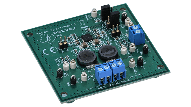
Evaluation Module for TPS65253 4.5V to 16V INPUT with 2 Buck Converters and Integrated FETS
Texas Instruments
Evaluation Module for TPS65253 4.5V to 16V INPUT with 2 Buck Converters and Integrated FETS
| Distributor | SKU | Stock | MOQ | 1 | 10 | 50 | 100 | 1,000 | 10,000 |
|---|---|---|---|---|---|---|---|---|---|
| DigiKey | 296-49346-ND | 1 | 1 | $248.75 | $248.75 | $248.75 | $248.75 | $248.75 | $248.75 |
| Arrow North American Components | TPS65253EVM | 0 | 1 | $270.34 | $267.63 | $262.31 | $259.68 | $251.97 | $249.45 |
| AVNET Express | TPS65253EVM | 0 | 1 | $96.38 | $96.38 | $96.38 | $96.38 | $96.38 | $96.38 |
| Mouser Electronics | 595-TPS65253EVM | 1 | 1 | $263.36 | $263.36 | $263.36 | $263.36 | $263.36 | $263.36 |
| Texas Instruments | TPS65253EVM | 11 | 1 | $199.00 | $199.00 | $199.00 | $199.00 | $199.00 | $199.00 |
| Verical Marketplace | TPS65253EVM | 28 | 1 | $81.79 | $91.42 | $89.11 | $89.11 | $89.11 | $89.11 |
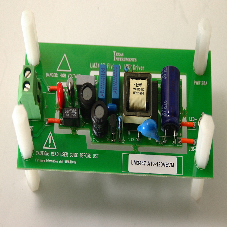
LM3447 Flyback Controller for LED Lighting Evaluation Module Board
Texas Instruments
LM3447 Flyback Controller for LED Lighting Evaluation Module Board
| Distributor | SKU | Stock | MOQ | 1 | 10 | 50 | 100 | 1,000 | 10,000 |
|---|---|---|---|---|---|---|---|---|---|
| DigiKey | 296-49207-ND | 1 | 1 | $118.80 | $118.80 | $118.80 | $118.80 | $118.80 | $118.80 |
| Arrow North American Components | LM3447-A19-120VEVM | 0 | 1 | $134.22 | $132.88 | $130.23 | $128.93 | $125.10 | $123.85 |
| AVNET Express | LM3447-A19-120VEVM | 0 | 1 | $120.78 | $120.78 | $120.78 | $120.78 | $120.78 | $120.78 |
| element14 APAC | LM3447-A19-120VEVM | 4 | 1 | * $122.88 | * $122.88 | * $122.88 | * $122.88 | * $122.88 | * $122.88 |
| Farnell | LM3447-A19-120VEVM | 4 | 1 | * $106.76 | * $106.76 | * $106.76 | * $106.76 | * $106.76 | * $106.76 |
| Mouser Electronics | 595-LM3447A19120VEVM | 2 | 1 | $128.71 | $128.71 | $128.71 | $128.71 | $128.71 | $128.71 |
| Newark | LM3447-A19-120VEVM | 4 | 1 | $0.00 | $0.00 | $0.00 | $0.00 | $0.00 | $0.00 |
| Texas Instruments | LM3447-A19-120VEVM | 30 | 1 | $99.00 | $99.00 | $99.00 | $99.00 | $99.00 | $99.00 |
| Verical Marketplace | LM3447-A19-120VEVM | 122 | 1 | $110.27 | $0.00 | $0.00 | $0.00 | $0.00 | $0.00 |
| Distributor | SKU | Stock | MOQ | 1 | 10 | 50 | 100 | 1,000 | 10,000 |
|---|---|---|---|---|---|---|---|---|---|
| DigiKey | P3Y103DKR-ND | 0 | $0.00 | $0.37 | $0.33 | $0.31 | $0.25 | $0.16 | |
| Future Electronics | EVM-3YSX50B14 | 2000 | $0.15 | ||||||
| Mouser Electronics | 667-EVM-3YSX50B14 | 0 | 1 |
TPS76933 evaluation module for SOT-23 LDO voltage regulator with 5-V to 3.3-V output power supply
Texas Instruments
TPS76933 evaluation module for SOT-23 LDO voltage regulator with 5-V to 3.3-V output power supply
| Distributor | SKU | Stock | MOQ | 1 | 10 | 50 | 100 | 1,000 | 10,000 |
|---|---|---|---|---|---|---|---|---|---|
| DigiKey | 296-11040-ND | 1 | 1 | $61.25 | $61.25 | $61.25 | $61.25 | $61.25 | $61.25 |
| Arrow North American Components | TPS76933EVM-127 | 0 | 1 | $66.57 | $65.90 | $64.59 | $63.94 | $62.04 | $61.42 |
| AVNET Europe | TPS76933EVM-127 | 0 | 1 | * $80.76 | * $84.69 | * $79.45 | * $76.83 | * $76.83 | * $76.83 |
| AVNET Express | TPS76933EVM-127 | 0 | 1 | $59.78 | $59.78 | $59.78 | $59.78 | $59.78 | $59.78 |
| Mouser Electronics | 595-TPS76933EVM-127 | 0 | 1 | $63.71 | $63.71 | $63.71 | $63.71 | $63.71 | $63.71 |
| Texas Instruments | TPS76933EVM-127 | 16 | 1 | $49.00 | $49.00 | $49.00 | $49.00 | $49.00 | $49.00 |
| Verical Marketplace | TPS76933EVM-127 | 28 | 1 | $55.35 | $55.35 | $55.35 | $55.35 | $55.35 | $55.35 |
| Win Source | TPS76933EVM-127 | 580 | 1 |