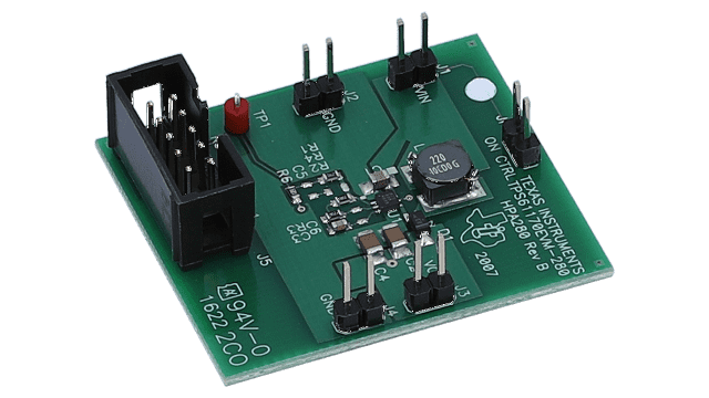
TPS61170 12V Input; 24V Output; 0.34A Evaluation Module
Texas Instruments
TPS61170 12V Input; 24V Output; 0.34A Evaluation Module
| Distributor | SKU | Stock | MOQ | 1 | 10 | 50 | 100 | 1,000 | 10,000 |
|---|---|---|---|---|---|---|---|---|---|
| DigiKey | 296-31229-ND | 0 | 1 | $58.80 | $58.80 | $58.80 | $58.80 | $58.80 | $58.80 |
| Arrow North American Components | TPS61170EVM-280 | 0 | 1 | $66.90 | $66.23 | $64.91 | $64.26 | $62.35 | $61.73 |
| AVNET Express | TPS61170EVM-280 | 0 | 1 | $59.78 | $59.78 | $59.78 | $59.78 | $59.78 | $59.78 |
| element14 APAC | TPS61170EVM-280 | 0 | 1 | * $76.33 | * $76.33 | * $76.33 | * $76.33 | * $76.33 | * $76.33 |
| Farnell | TPS61170EVM-280 | 0 | 1 | * $53.76 | * $53.76 | * $53.76 | * $53.76 | * $53.76 | * $53.76 |
| Mouser Electronics | 595-TPS61170EVM-280 | 6 | 1 | $63.71 | $63.71 | $63.71 | $63.71 | $63.71 | $63.71 |
| Newark | TPS61170EVM-280 | 0 | 6 | $50.73 | $50.73 | $50.73 | $50.73 | $50.73 | $50.73 |
| Texas Instruments | TPS61170EVM-280 | 37 | 1 | $49.00 | $49.00 | $49.00 | $49.00 | $49.00 | $49.00 |
| Verical Marketplace | TPS61170EVM-280 | 66 | 1 | $50.73 | $0.00 | $0.00 | $0.00 | $0.00 | $0.00 |
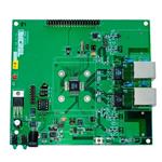
KSZ8852HLE-EVAL
Microchip Technology Inc.
Ethernet Development Tools Eval-2-Port Ethernet Controller
| Distributor | SKU | Stock | MOQ | 1 | 10 | 50 | 100 | 1,000 | 10,000 |
|---|---|---|---|---|---|---|---|---|---|
| DigiKey | 576-4519-ND | 0 | 1 | $345.00 | $345.00 | $345.00 | $345.00 | $345.00 | $345.00 |
| MicrochipDirect | KSZ8852HLE-EVAL | 12 | $345.00 | $345.00 | $345.00 | $345.00 | $345.00 | $345.00 | |
| Mouser Electronics | 998-KSZ8852HLE-EVAL | 0 | 1 |
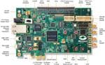
M2S090TS-EVAL-KIT
Microchip Technology Inc.
Programmable Logic IC Development Tools SmartFusion2 Security Eval Kit
| Distributor | SKU | Stock | MOQ | 1 | 10 | 50 | 100 | 1,000 | 10,000 |
|---|---|---|---|---|---|---|---|---|---|
| DigiKey | 1100-1228-ND | 219 | 1 | $720.02 | $720.02 | $720.02 | $720.02 | $720.02 | $720.02 |
| Arrow North American Components | M2S090TS-EVAL-KIT | 0 | 1 | $679.27 | $406.86 | $398.02 | $394.10 | $382.34 | $379.36 |
| AVNET Asia Pacific | M2S090TS-EVAL-KIT | 0 | 1 | $0.00 | $0.00 | $0.00 | $0.00 | $0.00 | $0.00 |
| AVNET Europe | M2S090TS-EVAL-KIT | 0 | 1 | * $477.75 | * $477.75 | * $477.75 | * $477.75 | * $477.75 | * $477.75 |
| AVNET Express | M2S090TS-EVAL-KIT | 0 | 1 | $707.99 | $689.92 | $684.02 | $684.02 | $684.02 | $684.02 |
| Farnell | M2S090TS-EVAL-KIT | 2 | 1 | * $731.82 | * $731.82 | * $731.82 | * $731.82 | * $731.82 | * $731.82 |
| Mouser Electronics | 494-M2S090TSEVAL-KIT | 36 | 1 | $780.08 | $780.08 | $780.08 | $780.08 | $780.08 | $780.08 |
| Newark | M2S090TS-EVAL-KIT | 1 | 1 | $705.65 | $705.65 | $705.65 | $705.65 | $705.65 | $705.65 |
| Verical Marketplace | M2S090TS-EVAL-KIT | 1 | 1 | $928.82 | $928.82 | $928.82 | $928.82 | $928.82 | $928.82 |
| Distributor | SKU | Stock | MOQ | 1 | 10 | 50 | 100 | 1,000 | 10,000 |
|---|---|---|---|---|---|---|---|---|---|
| Mouser Electronics | 700-MAX5393EVMINIQU+ | 0 | 1 |
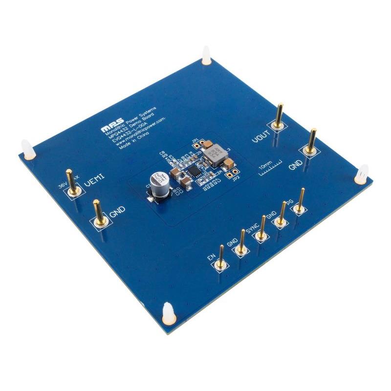
EVQ4432-L-00A
Monolithic Power Systems (MPS)
MPQ4432, MPQ4432-AEC1 - 1 Non-Isolated Output DC/DC, Step Down Evaluation Board
| Distributor | SKU | Stock | MOQ | 1 | 10 | 50 | 100 | 1,000 | 10,000 |
|---|---|---|---|---|---|---|---|---|---|
| DigiKey | 1589-EVQ4432-L-00A-ND | 1 | 1 | $51.27 | $51.27 | $51.27 | $51.27 | $51.27 | $51.27 |
| AVNET Express | EVQ4432-L-00A | 0 | 1 | $57.20 | $51.40 | $50.00 | $50.00 | $50.00 | $50.00 |
| Mouser Electronics | 946-EVQ4432-L-00A | 0 | 1 | $51.75 | $51.75 | $51.75 | $51.75 | $51.75 | $51.75 |
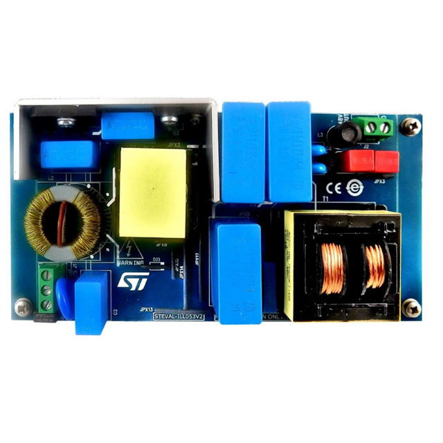
| Distributor | SKU | Stock | MOQ | 1 | 10 | 50 | 100 | 1,000 | 10,000 |
|---|---|---|---|---|---|---|---|---|---|
| DigiKey | 497-18363-ND | 1 | 1 | $133.61 | $133.61 | $133.61 | $133.61 | $133.61 | $133.61 |
| Arrow North American Components | STEVAL-ILL053V2 | 4 | 1 | $28.60 | $28.60 | $28.60 | $28.60 | $28.60 | $28.60 |
| AVNET Europe | STEVAL-ILL053V2 | 0 | 1 | * $0.00 | * $0.00 | * $0.00 | * $0.00 | * $0.00 | * $0.00 |
| AVNET Express | STEVAL-ILL053V2 | 5 | 1 | $0.00 | $0.00 | $0.00 | $0.00 | $0.00 | $0.00 |
| element14 APAC | STEVAL-ILL053V2 | 1 | 1 | * $145.93 | * $145.93 | * $145.93 | * $145.93 | * $145.93 | * $145.93 |
| Farnell | STEVAL-ILL053V2 | 1 | 1 | * $135.31 | * $135.31 | * $135.31 | * $135.31 | * $135.31 | * $135.31 |
| Future Electronics | STEVAL-ILL053V2 | 5 | 1 | $133.35 | |||||
| Mouser Electronics | 511-STEVAL-ILL053V2 | 5 | 1 | $142.52 | $142.52 | $142.52 | $142.52 | $142.52 | $142.52 |
| Newark | STEVAL-ILL053V2 | 2 | 1 | $158.04 | $158.04 | $158.04 | $158.04 | $158.04 | $158.04 |
| RS Components | STEVAL-ILL053V2 | 0 | $131.06 | ||||||
| RS Components (APAC) | STEVAL-ILL053V2 | 0 | $264.55 | ||||||
| Verical Marketplace | STEVAL-ILL053V2 | 4 | 1 | $28.60 | $28.60 | $28.60 | $28.60 | $28.60 | $28.60 |
| Win Source | STEVAL-ILL053V2 | 1 | 1 |
MICROFJ-SMTPA-30035-GEVB
onsemi
MicroFJ-30035 J-SERIES SIPM Light, Silicon Photomultiplier (SiPM) Sensor Evaluation Board
| Distributor | SKU | Stock | MOQ | 1 | 10 | 50 | 100 | 1,000 | 10,000 |
|---|---|---|---|---|---|---|---|---|---|
| DigiKey | MICROFJ-SMTPA-30035-GEVBOS-ND | 0 | 1 | $82.25 | $82.06 | $82.06 | $82.06 | $82.06 | $82.06 |
| Arrow North American Components | MICROFJ-SMTPA-30035-GEVB | 0 | 1 | $88.12 | $87.24 | $85.51 | $84.65 | $82.14 | $81.31 |
| AVNET Asia Pacific | MICROFJ-SMTPA-30035-GEVB | 0 | 1 | $85.53 | $82.28 | $80.25 | $80.25 | $80.25 | |
| AVNET Europe | MICROFJ-SMTPA-30035-GEVB | 0 | 1 | * $114.76 | * $111.98 | * $103.63 | * $98.76 | * $98.76 | * $98.76 |
| AVNET Express | MICROFJ-SMTPA-30035-GEVB | 0 | 1 | $87.84 | $84.42 | $83.33 | $80.25 | $80.25 | |
| element14 APAC | MICROFJ-SMTPA-30035-GEVB | 1 | 1 | * $93.64 | * $89.89 | * $88.02 | * $88.02 | * $88.02 | * $88.02 |
| Farnell | MICROFJ-SMTPA-30035-GEVB | 1 | 1 | * $96.85 | * $92.99 | * $91.04 | * $91.04 | * $91.04 | * $91.04 |
| Mouser Electronics | 863-MFJSMTPA30035EVB | 0 | 1 | $84.09 | $84.09 | $84.09 | $84.09 | $84.09 | $84.09 |
| Newark | MICROFJ-SMTPA-30035-GEVB | 1 | 1 | $87.78 | $84.52 | $84.52 | $84.52 | $84.52 | $84.52 |
| RS Components | MICROFJ-SMTPA-30035-GEVB | 0 | $83.04 | ||||||
| RS Components (APAC) | MICROFJ-SMTPA-30035-GEVB | 0 | $139.94 |
| Distributor | SKU | Stock | MOQ | 1 | 10 | 50 | 100 | 1,000 | 10,000 |
|---|---|---|---|---|---|---|---|---|---|
| DigiKey | S12VR32EVB-ND | 0 | $132.70 | $132.70 | $132.70 | $132.70 | $132.70 | $132.70 | |
| Ameya360 | S12VR32EVB | 1 | $113.37 | $113.37 | $113.37 | $113.37 | $113.37 | $113.37 | |
| AVNET Express | S12VR32EVB | 0 | 1 | $128.63 | $121.80 | $120.74 | $120.74 | $120.74 | $120.74 |
| element14 APAC | S12VR32EVB | 8 | 1 | * $160.35 | * $160.35 | * $160.35 | * $160.35 | * $160.35 | * $160.35 |
| Farnell | S12VR32EVB | 4 | 1 | * $149.25 | * $149.25 | * $149.25 | * $149.25 | * $149.25 | * $149.25 |
| Future Electronics | S12VR32EVB | 1 | 1 | $55.00 | $55.00 | $55.00 | $55.00 | $55.00 | $55.00 |
| Mouser Electronics | 841-S12VR32EVB | 4 | 1 | $137.44 | $137.44 | $137.44 | $137.44 | $137.44 | $137.44 |
| Newark | S12VR32EVB | 8 | 1 | $146.48 | $146.48 | $146.48 | $146.48 | $146.48 | $146.48 |
| Win Source | S12VR32EVB | 6300 |
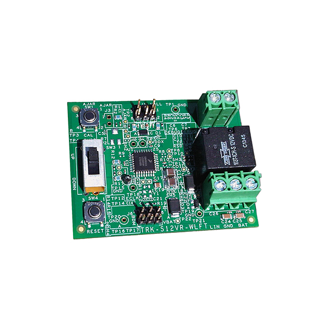
| Distributor | SKU | Stock | MOQ | 1 | 10 | 50 | 100 | 1,000 | 10,000 |
|---|---|---|---|---|---|---|---|---|---|
| DigiKey | 568-13526-ND | 21 | 1 | $1,025.88 | $1,025.88 | $1,025.88 | $1,025.88 | $1,025.88 | $1,025.88 |
| Ameya360 | SBC-S32V234 | 0 | $931.36 | $931.36 | $931.36 | $931.36 | $931.36 | $931.36 | |
| Arrow North American Components | SBC-S32V234 | 0 | 1 | $1,067.68 | $1,067.68 | $1,067.68 | $1,067.68 | $1,067.68 | $1,067.68 |
| AVNET Asia Pacific | SBC-S32V234 | 0 | 1 | $1,094.93 | $1,027.35 | $1,027.35 | $1,027.35 | $1,027.35 | $1,027.35 |
| AVNET Europe | SBC-S32V234 | 1 | 1 | * $3,302.09 | * $3,062.81 | * $2,344.97 | * $2,124.83 | * $2,124.83 | * $2,124.83 |
| AVNET Express | SBC-S32V234 | 3 | 1 | $1,081.60 | $1,081.60 | $1,081.60 | $1,081.60 | $1,081.60 | $1,081.60 |
| element14 APAC | SBC-S32V234 | 15 | 1 | * $1,130.67 | * $1,130.67 | * $1,130.67 | * $1,130.67 | * $1,130.67 | * $1,130.67 |
| Farnell | SBC-S32V234 | 14 | 1 | * $996.02 | * $996.02 | * $996.02 | * $996.02 | * $996.02 | * $996.02 |
| Future Electronics | SBC-S32V234 | 2 | 1 | $649.00 | $649.00 | $649.00 | $649.00 | $649.00 | $649.00 |
| Mouser Electronics | 771-SBC-S32V234 | 1 | 1 | $1,081.86 | $1,081.86 | $1,081.86 | $1,081.86 | $1,081.86 | $1,081.86 |
| Newark | SBC-S32V234 | 1 | 1 | $1,382.08 | $1,382.08 | $1,382.08 | $1,382.08 | $1,382.08 | $1,382.08 |
| Verical Marketplace | SBC-S32V234 | 1 | 1 | $1,091.55 | $1,091.55 | $1,091.55 | $1,091.55 | $1,091.55 | $1,091.55 |
| Win Source | SBC-S32V234 | 3930 |
KITVALVECNTLEVM
NXP Semiconductors N.V.
MC34SB0800 MC34SB0410 - Motor Controller/Driver Power Management Evaluation Board
| Distributor | SKU | Stock | MOQ | 1 | 10 | 50 | 100 | 1,000 | 10,000 |
|---|---|---|---|---|---|---|---|---|---|
| DigiKey | KITVALVECNTLEVM-ND | 0 | 1 | $441.97 | $441.97 | $441.97 | $441.97 | $441.97 | $441.97 |
| Arrow North American Components | KITVALVECNTLEVM | 0 | 1 | $495.79 | $490.83 | $481.07 | $476.26 | $462.11 | $457.49 |
| AVNET Express | KITVALVECNTLEVM | 0 | 1 | $266.56 | $262.48 | $261.12 | $261.12 | $261.12 | $261.12 |
| element14 APAC | KITVALVECNTLEVM | 1 | 1 | * $263.16 | * $263.16 | * $263.16 | * $263.16 | * $263.16 | * $263.16 |
| Farnell | KITVALVECNTLEVM | 1 | 1 | * $242.11 | * $242.11 | * $242.11 | * $242.11 | * $242.11 | * $242.11 |
| Mouser Electronics | 841-KITVALVECNTLEVM | 3 | 1 | $300.15 | $300.15 | $300.15 | $300.15 | $300.15 | $300.15 |
| Newark | KITVALVECNTLEVM | 6 | 1 | $398.60 | $398.60 | $398.60 | $398.60 | $398.60 | $398.60 |
| Verical Marketplace | KITVALVECNTLEVM | 6 | 1 | $557.48 | $506.12 | $506.12 | $506.12 | $506.12 | $506.12 |