FMFRMARM
Fairview Microwave
Non-Penetrating Antenna Flat Roof Mount 34-Inch Pole Only |Fairview Microwave FMFRMARM
| Distributor | SKU | Stock | MOQ | 1 | 10 | 50 | 100 | 1,000 | 10,000 |
|---|---|---|---|---|---|---|---|---|---|
| DigiKey | 5328-FMFRMARM-ND | 0 | 1 | $108.00 | $108.00 | $108.00 | $108.00 | $108.00 | $108.00 |
| Newark | FMFRMARM | 12 | 1 | $108.00 | $108.00 | $108.00 | $108.00 | $108.00 | $108.00 |
| Distributor | SKU | Stock | MOQ | 1 | 10 | 50 | 100 | 1,000 | 10,000 |
|---|---|---|---|---|---|---|---|---|---|
| DigiKey | BEF-MWS120-ARM | 2 | 1 | $362.05 | $362.05 | $362.05 | $362.05 | $362.05 | $362.05 |
| element14 APAC | BEF-MWS120-ARM | 0 | 1 | * $363.02 | * $342.35 | * $328.37 | * $328.37 | * $328.37 | * $328.37 |
| Farnell | BEF-MWS120-ARM | 0 | 1 | * $268.72 | * $257.97 | * $247.23 | * $247.23 | * $247.23 | * $247.23 |
| Newark | BEF-MWS120-ARM | 0 | 1 | $467.53 | $375.51 | $320.77 | $320.77 | $320.77 | $320.77 |
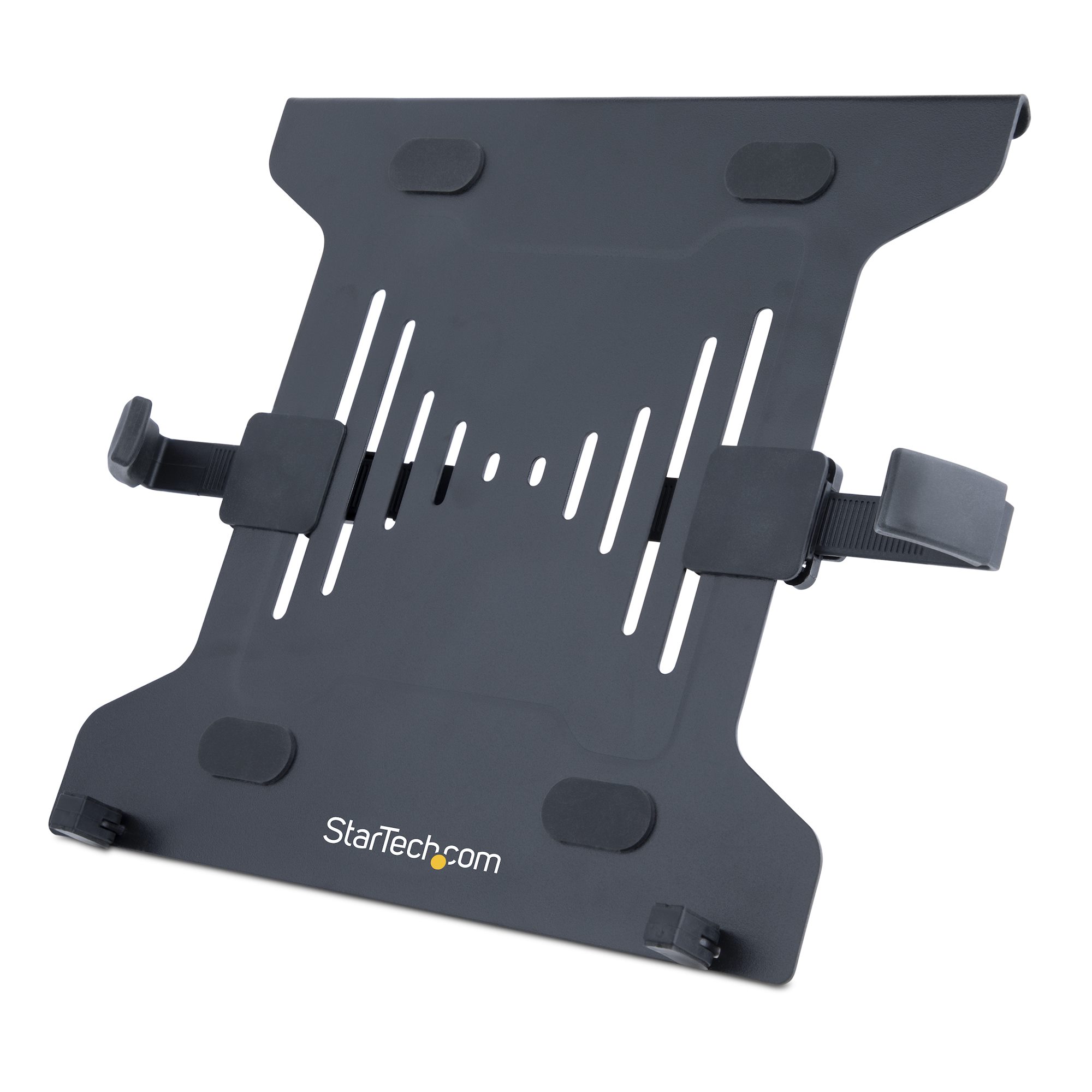
| Distributor | SKU | Stock | MOQ | 1 | 10 | 50 | 100 | 1,000 | 10,000 |
|---|---|---|---|---|---|---|---|---|---|
| DigiKey | LAPTOP-ARM-TRAY | 5 | 1 | $50.93 | $45.17 | $41.55 | $40.08 | $38.21 | $38.21 |
| Farnell | LAPTOP-ARM-TRAY | 1 | 1 | * $48.06 | * $48.06 | * $48.06 | * $48.06 | * $48.06 | * $48.06 |
| Newark | LAPTOP-ARM-TRAY | 1 | 1 | $62.17 | $62.17 | $62.17 | $62.17 | $62.17 | $62.17 |

FARM1C21
Vicor UK
Filter/Autoranging Rectifier Module 90V to 132V/180V to 264V 250V to 370V Screw Mount 9-Pin Half Brick
| Distributor | SKU | Stock | MOQ | 1 | 10 | 50 | 100 | 1,000 | 10,000 |
|---|---|---|---|---|---|---|---|---|---|
| DigiKey | FARM1C21-ND | 15 | 1 | $356.52 | $283.20 | $258.40 | $258.40 | $258.40 | $258.40 |
| Ameya360 | FARM1C21 | 0 | $204.48 | $204.48 | $204.48 | $204.48 | $204.48 | $204.48 | |
| Arrow North American Components | FARM1C21 | 0 | 1 | $270.25 | $0.00 | $0.00 | $0.00 | $0.00 | $0.00 |
| AVNET Express | FARM1C21 | 0 | 1 | $273.00 | $266.13 | $253.08 | $253.08 | $253.08 | $253.08 |
FARM1T23
Vicor UK
Filter/Autoranging Rectifier Module 90V to 132V/180V to 264V 250V to 370V Through Hole 9-Pin Half Brick
| Distributor | SKU | Stock | MOQ | 1 | 10 | 50 | 100 | 1,000 | 10,000 |
|---|---|---|---|---|---|---|---|---|---|
| DigiKey | 1102-FARM1T23-ND | 0 | 1 | $363.98 | $363.98 | $363.98 | $363.98 | $363.98 | $363.98 |
| Ameya360 | FARM1T23 | 0 | $215.98 | $215.98 | $215.98 | $215.98 | $215.98 | $215.98 | |
| Arrow North American Components | FARM1T23 | 0 | 1 | $275.90 | $0.00 | $0.00 | $0.00 | $0.00 | $0.00 |
| AVNET Express | FARM1T23 | 0 | 1 | $278.70 | $271.70 | $258.36 | $258.36 | $258.36 | $258.36 |
FARM1TG1
Vicor UK
Filter/Autoranging Rectifier Module 90V to 132V/180V to 264V 250V to 370V Screw Mount 9-Pin Half Brick
| Distributor | SKU | Stock | MOQ | 1 | 10 | 50 | 100 | 1,000 | 10,000 |
|---|---|---|---|---|---|---|---|---|---|
| DigiKey | 1102-FARM1TG1-ND | 13 | 1 | $372.74 | $296.07 | $270.15 | $270.15 | $270.15 | $270.15 |
| Arrow North American Components | FARM1TG1 | 0 | 1 | $282.53 | $0.00 | $0.00 | $0.00 | $0.00 | $0.00 |
| AVNET Express | FARM1TG1 | 0 | 1 | $297.39 | $285.71 | $264.58 | $264.58 | $264.58 | $264.58 |
FARM1TN2
Vicor UK
Filter/Autoranging Rectifier Module 90V to 132V/180V to 264V 250V to 370V Screw Mount 9-Pin Half Brick
| Distributor | SKU | Stock | MOQ | 1 | 10 | 50 | 100 | 1,000 | 10,000 |
|---|---|---|---|---|---|---|---|---|---|
| DigiKey | 1102-FARM1TN2-ND | 0 | 1 | $377.09 | $377.09 | $377.09 | $377.09 | $377.09 | $377.09 |
| AVNET Express | FARM1TN2 | 0 | 1 | $369.55 | $289.06 | $267.68 | $267.68 | $267.68 | $267.68 |
FARM2C23
Vicor UK
Filter/Autoranging Rectifier Module 90V to 132V/180V to 264V 250V to 370V Through Hole 9-Pin Half Brick
| Distributor | SKU | Stock | MOQ | 1 | 10 | 50 | 100 | 1,000 | 10,000 |
|---|---|---|---|---|---|---|---|---|---|
| DigiKey | FARM2C23-ND | 0 | 1 | $368.84 | $292.98 | $267.33 | $267.33 | $267.33 | $267.33 |
| Ameya360 | FARM2C23 | 0 | $205.58 | $205.58 | $205.58 | $205.58 | $205.58 | $205.58 | |
| Arrow North American Components | FARM2C23 | 0 | 1 | $279.58 | $0.00 | $0.00 | $0.00 | $0.00 | $0.00 |
| AVNET Express | FARM2C23 | 0 | 1 | $282.43 | $275.32 | $261.81 | $261.81 | $261.81 | $261.81 |
FARM2CF2
Vicor UK
Filter/Autoranging Rectifier Module 90V to 132V/180V to 264V 250V to 370V Screw Mount 9-Pin Half Brick
| Distributor | SKU | Stock | MOQ | 1 | 10 | 50 | 100 | 1,000 | 10,000 |
|---|---|---|---|---|---|---|---|---|---|
| DigiKey | 1102-FARM2CF2-ND | 0 | 1 | $357.41 | $357.41 | $357.41 | $357.41 | $357.41 | $357.41 |
| Ameya360 | FARM2CF2 | 0 | $208.36 | $208.36 | $208.36 | $208.36 | $208.36 | $208.36 | |
| AVNET Express | FARM2CF2 | 0 | 1 | $350.26 | $273.96 | $253.70 | $253.70 | $253.70 | $253.70 |
FARM1C23
Vicor UK
Filter/Autoranging Rectifier Module 90V to 132V/180V to 264V 250V to 370V Through Hole 9-Pin Half Brick
| Distributor | SKU | Stock | MOQ | 1 | 10 | 50 | 100 | 1,000 | 10,000 |
|---|---|---|---|---|---|---|---|---|---|
| DigiKey | 1102-FARM1C23-ND | 0 | 1 | $359.83 | $359.83 | $359.83 | $359.83 | $359.83 | $359.83 |
| AVNET Express | FARM1C23 | 0 | 1 | $352.63 | $278.68 | $259.51 | $255.43 | $255.43 | $255.43 |