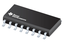
SN74LS112ANSRE4

Texas Instruments
Category: Logic
These devices contain two independent J-K negative-edge-triggered flip-flops. A low level at the preset and clear inputs sets or resets the outputs regardless of the levels of the other inputs. When preset and clear are inactive (high), data at the J and K inputs meeting the setup time requirements are transferred to the outputs on the negative-going edge of the clock pulse. Clock triggering occurs at a voltage level and is not directly related to the rise time of the clock pulse. Following the hold time interval, data at the J and K inputs may be changed without affecting the levels at the outputs. These versatile flip-flops can perform as toggle flip-flops by tying J and K high.
The SN54LS112A and SN54S112 are characterized for operation over the full military temperature range of -55°C to 125°C. The SN74LS112A and SN74S112A are characterized for operation from 0°C to 70°C.
$0.79Distributors
Parts in family
Technical Specifications
| Lead Free Status | No |
| ROHS Compliance | Compliant |
| Approx. Price (US$) | 0.41 | 1ku |
| Bits(#) | 2 |
| Estimated Package Size (WxL)(mm2) | [pf]16SO[/pf] |
| F @ Nom Voltage(Max)(Mhz) | 35 |
| ICC @ Nom Voltage(Max)(mA) | 6 |
| Input Type | TTL |
| Output Drive (IOL/IOH)(Max)(mA) | -0.4/8 |
| Output Type | TTL |
| Package Group | PDIP,SO,SOIC |
| Rating | Catalog |
| Schmitt Trigger | No |
| Technology Family | LS |
| VCC(Max)(V) | 5.25 |
| VCC(Min)(V) | 4.75 |
| Voltage(Nom)(V) | 5 |
| tpd @ Nom Voltage(Max)(ns) | 20 |


