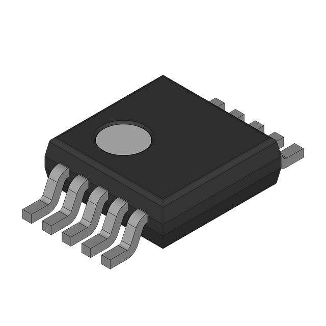
AD9434BCPZ-500
Analog Devices Inc.
The AD9434 is a 12-bit monolithic sampling analog-to-digital converter (ADC) optimized for high performance, low power, and ease of use. The part operates at up to a 500 MSPS conversion rate and is optimized for outstanding dynamic performance in wideband carrier and broadband systems. All necessary functions, including a sample-and-hold and voltagereference, are included on the chip to provide a complete signal conversion solution. The VREF pin can be used to monitor the internal reference or provide an external voltage reference (external reference mode must be enabled through the SPI port). The ADC requires a 1.8 V analog voltage supply and a differential clock for full performance operation. The digital outputs are LVDS (ANSI-644) compatible and support twos complement, offset binary format, or Gray code. A data clock output is available for proper output data timing.Fabricated on an advanced BiCMOS process, the AD9434 isavailable in a 56-lead LFCSP, specified over the industrial temperature range (−40°C to +85°C). This part is protected under a U.S. patent.APPLICATIONS Wireless and wired broadband communications Cable reverse path Communications test equipment Radar and satellite subsystems Power amplifier linearizationPRODUCT HIGHLIGHTS High Performance. Maintains 65 dBFS SNR at 500 MSPS with a 250 MHz input. Low Power. Consumes only 660 mW at 500 MSPS. Ease of Use. LVDS output data and output clock signal allow interface to current FPGA technology. The on-chip reference and sample and hold provide flexibility in system design. Use of a single 1.8 V supply simplifies system power supply design. Serial Port Control. Standard serial port interface supports various product functions, such as data formatting, power-down, gain adjust, and output test pattern generation. The AD9434 is pin compatible with the AD9230, and can be substituted in many applications with minimal design changes.
Distributor | SKU | Stock | MOQ | 1 | 10 | 50 | 100 | 1,000 | 10,000 |
---|---|---|---|---|---|---|---|---|---|
DigiKey | AD9434BCPZ-500 | 39 | $181.60 | $173.93 | $173.93 | $173.93 | $173.93 | $173.93 | |
Analog Devices Inc | AD9434BCPZ-500 | 0 | $260.19 | $259.29 | $259.29 | $259.29 | $259.29 | $259.29 | |
element14 APAC | AD9434BCPZ-500 | 2 | 1 | * $459.82 | * $456.78 | * $456.78 | * $456.78 | * $456.78 | * $456.78 |
Farnell | AD9434BCPZ-500 | 2 | 1 | * $196.47 | * $196.47 | * $196.47 | * $196.47 | * $196.47 | * $196.47 |
Mouser Electronics | AD9434BCPZ-500 | 4 | 1 | $242.15 | $223.62 | $223.62 | $223.62 | $223.62 | $223.62 |
Newark | AD9434BCPZ-500 | 2 | 1 | $218.57 | $211.77 | $210.81 | $210.81 | $210.81 | $210.81 |
Win Source | AD9434BCPZ-500 | 1070 | 1 | $152.73 | $134.11 | $134.11 | $134.11 | $134.11 | $134.11 |
AD9484-500EBZ
Analog Devices Inc.
The AD9484 is an 8-bit, monolithic, sampling analog-to-digital converter (ADC) optimized for high performance, low power, and ease of use. The part operates at up to a 500 MSPS conversion rate and is optimized for outstanding dynamic performance in wideband carrier and broadband systems. All necessary functions, including a sample-and-hold and voltage reference, are included on the chip to provide a complete signal conversion solution. The VREF pin can be used to monitor the internal reference or provide an external voltage reference (external reference mode must be enabled through the SPI port).The ADC requires a 1.8 V analog voltage supply and a differential clock for full performance operation. The digital outputs are LVDS (ANSI-644) compatible and support twos complement, offset binary format, or Gray code. A data clock output is available for proper output data timing.Fabricated on an advanced BiCMOS process, the AD9484 is available in a 56-lead LFCSP, and is specified over the industrial temperature range (−40°C to +85°C). This product is protected under U.S. and international patents.PRODUCT HIGHLIGHTS High Performance. Maintains 47 dBFS SNR at 500 MSPS with a 250 MHz input. Ease of Use. LVDS output data and output clock signal allow interface to current FPGA technology. The on-chip reference and sample and hold provide flexibility in system design. Use of a single 1.8 V supply simplifies system power supply design. Serial Port Control. Standard serial port interface supports various product functions, such as data formatting, disabling the clock duty cycle stabilizer, power down, gain adjust, and output test pattern generation.APPLICATIONS Wireless and wired broadband communications Cable reverse path Communications test equipment Low cost digital oscilloscopes Satellite subsystems Power amplifier linearization
Distributor | SKU | Stock | MOQ | 1 | 10 | 50 | 100 | 1,000 | 10,000 |
---|---|---|---|---|---|---|---|---|---|
DigiKey | AD9484-500EBZ | 1 | $312.34 | $312.34 | $312.34 | $312.34 | $312.34 | $312.34 | |
Analog Devices Inc | AD9484-500EBZ | 0 | $307.20 | $307.20 | $307.20 | $307.20 | $307.20 | $307.20 | |
Mouser Electronics | AD9484-500EBZ | 3 | 1 | $332.82 | $332.82 | $332.82 | $332.82 | $332.82 | $332.82 |
AD9508BCPZ-REEL7
Analog Devices Inc.
The AD9508 provides clock fanout capability in a design thatemphasizes low jitter to maximize system performance. Thisdevice benefits applications like clocking data converters withdemanding phase noise and low jitter requirements.There are four independent differential clock outputs, each withvarious types of logic levels available. Available logic typesinclude LVDS (1.65 GHz), HSTL (1.65 GHz), and 1.8 V CMOS(250 MHz). In 1.8 V CMOS output mode, the differential outputbecomes two CMOS single-ended signals. The CMOS outputsare 1.8 V logic levels, regardless of the operating supply voltage.Each output has a programmable divider that can be bypassedor be set to divide by any integer up to 1024. In addition, theAD9508 supports a coarse output phase adjustment betweenthe outputs.The device can also be pin programmed for various fixedconfigurations at power-up without the need for SPI or I2C programming.The AD9508 is available in a 24-lead LFCSP and operates froma either a single 2.5 V or 3.3 V supply. The temperature range is−40°C to +85°C.Applications Low jitter, low phase noise clock distribution Clocking high speed ADCs, DACs, DDSs, DDCs, DUCs, MxFEs High performance wireless transceivers High performance instrumentation Broadband infrastructure
Distributor | SKU | Stock | MOQ | 1 | 10 | 50 | 100 | 1,000 | 10,000 |
---|---|---|---|---|---|---|---|---|---|
DigiKey | AD9508BCPZ-REEL7 | 403 | $14.40 | $10.01 | $8.86 | $7.57 | $5.90 | $7.45 | |
Analog Devices Inc | AD9508BCPZ-REEL7 | 0 | $13.27 | $12.19 | $11.69 | $10.30 | $9.16 | $9.16 | |
Arrow North American Components | AD9508BCPZ-REEL7 | 62 | 1 | $9.23 | $8.34 | $7.92 | $7.92 | $7.92 | $7.92 |
element14 APAC | AD9508BCPZ-REEL7 | 1039 | 1 | * $20.50 | * $19.07 | * $18.36 | * $17.64 | * $16.93 | * $16.93 |
Farnell | AD9508BCPZ-REEL7 | 1039 | 1 | * $10.90 | * $8.10 | * $7.85 | * $7.45 | * $7.30 | * $7.30 |
Mouser Electronics | AD9508BCPZ-REEL7 | 1512 | 1 | $9.76 | $8.81 | $8.40 | $6.96 | $5.53 | $5.34 |
Newark | AD9508BCPZ-REEL7 | 1154 | 1 | $10.35 | $9.15 | $8.70 | $8.70 | $8.70 | $8.70 |
Verical Marketplace | AD9508BCPZ-REEL7 | 62 | 2 | $8.34 | $7.92 | $7.92 | $7.92 | $7.92 | |
Win Source | AD9508BCPZ-REEL7 | 29206 | 4 | $13.07 | $10.82 | $10.82 | $10.82 | $10.82 |
AD9557/PCBZ
Analog Devices Inc.
The AD9557 is a low loop bandwidth clock multiplier that provides jitter cleanup and synchronization for many systems, including synchronous optical networks (OTN/SONET/SDH). The AD9557 generates an output clock synchronized to up to four external input references. The digital PLL allows for reduction of input time jitter or phase noise associated with the external references. The digitally controlled loop and holdover circuitry of the AD9557 continuously generates a low jitter output clock even when all reference inputs have failed.The AD9557 operates over an industrial temperature range of −40°C to +85°C. If more inputs/outputs are needed, refer to the AD9558 for the four-input/six-output version of the samedevice.Applications Network synchronization, including synchronous Ethernet and SDH to OTN mapping/demapping Cleanup of reference clock jitter SONET/SDH/OTN clocks up to 100 Gbps, including FEC Stratum 3 holdover, jitter cleanup, and phase transient control Wireless base station controllers Cable infrastructure Data communications
Distributor | SKU | Stock | MOQ | 1 | 10 | 50 | 100 | 1,000 | 10,000 |
---|---|---|---|---|---|---|---|---|---|
DigiKey | AD9557/PCBZ | 0 | 1 | $247.95 | $247.95 | $247.95 | $247.95 | $247.95 | $247.95 |
Analog Devices Inc | AD9557/PCBZ | 0 | $265.31 | $265.31 | $265.31 | $265.31 | $265.31 | $265.31 | |
Arrow North American Components | AD9557/PCBZ | 0 | 1 | $215.62 | $215.62 | $215.62 | $215.62 | $215.62 | $215.62 |
Mouser Electronics | AD9557/PCBZ | 3 | 1 | $274.57 | $274.57 | $274.57 | $274.57 | $274.57 | $274.57 |
Newark | AD9557/PCBZ | 0 | $206.63 | $206.63 | $206.63 | $206.63 | $206.63 | $206.63 | |
Verical Marketplace | AD9557/PCBZ | 13 | 1 | $283.37 | $268.05 | $268.05 | $268.05 | $268.05 | $268.05 |
AD9633-125EBZ
Analog Devices Inc.
The AD9633 is a quad, 12-bit, 80 MSPS/105 MSPS/125 MSPS analog-to-digital converter (ADC) with an on-chip sample-and-hold circuit designed for low cost, low power, small size, and ease of use. The product operates at a conversion rate of up to 125 MSPS and is optimized for outstanding dynamic performance and low power in applications where a small package size is critical.The ADC requires a single 1.8 V power supply and LVPECL-/CMOS-/LVDS-compatible sample rate clock for full performance operation. No external reference or driver components are required for many applications.The ADC automatically multiplies the sample rate clock for the appropriate LVDS serial data rate. A data clock output (DCO) for capturing data on the output and a frame clock output (FCO) for signaling a new output byte are provided. Individual-channel power-down is supported and typically consumes less than 2 mW when all channels are disabled.The ADC contains several features designed to maximize flexibility and minimize system cost, such as programmable output clock and data alignment and digital test pattern generation. The available digital test patterns include built-in deterministic and pseudorandom patterns, along with custom user-defined test patterns entered via the serial port interface (SPI).The AD9633 is available in a RoHS-compliant, 48-lead LFCSP. It is specified over the industrial temperature range of −40°C to +85°C. This product is protected by a U.S. patent. Applications Medical ultrasound High speed imaging Quadrature radio receivers Diversity radio receivers Test equipment
Distributor | SKU | Stock | MOQ | 1 | 10 | 50 | 100 | 1,000 | 10,000 |
---|---|---|---|---|---|---|---|---|---|
DigiKey | AD9633-125EBZ | 3 | $274.59 | $274.59 | $274.59 | $274.59 | $274.59 | $274.59 | |
Analog Devices Inc | AD9633-125EBZ | 0 | $335.12 | $335.12 | $335.12 | $335.12 | $335.12 | $335.12 | |
Mouser Electronics | AD9633-125EBZ | 3 |
AD9634-250EBZ
Analog Devices Inc.
The AD9634 is a 12-bit, analog-to-digital converter (ADC) with sampling speeds of up to 250 MSPS. The AD9634 is designed to support communications applications where low cost, small size, wide bandwidth, and versatility are desired.The ADC core features a multistage, differential pipelined architecture with integrated output error correction logic. The ADC features wide bandwidth inputs that can support a variety of user-selectable input ranges. An integrated voltage reference eases design considerations. A duty cycle stabilizer (DCS) is provided to compensate for variations in the ADC clock duty cycle, allowing the converter to maintain excellent performance.The ADC output data are routed directly to the external 12-bit LVDS output port.Flexible power-down options allow significant power savings, when desired.Programming for setup and control is accomplished using a 3-wire, SPI-compatible serial interface.The AD9634 is available in a 32-lead LFCSP and is specified over the industrial temperature range of −40°C to +85°C. This product is protected by a U.S. patent.PRODUCT HIGHLIGHTS Integrated 12-bit, 170 MSPS/210 MSPS/250 MSPS ADC. Fast overrange and threshold detect. Proprietary differential input maintains excellent SNR performance for input frequencies up to 350 MHz. 3-pin, 1.8V SPI port for register programming and readback. Pin compatibility with the AD9642, allowing a simple migration up to 14 bits, and with the AD6672. APPLICATIONS Communications Diversity radio systems Multimode digital receivers (3G) TD-SCDMA, WiMax, WCDMA, CDMA2000, GSM, EDGE, LTE I/Q demodulation systems Smart antenna systems General-purpose software radios Ultrasound equipment Broadband data applications
Distributor | SKU | Stock | MOQ | 1 | 10 | 50 | 100 | 1,000 | 10,000 |
---|---|---|---|---|---|---|---|---|---|
DigiKey | AD9634-250EBZ | 2 | $384.00 | $384.00 | $384.00 | $384.00 | $384.00 | $384.00 | |
Analog Devices Inc | AD9634-250EBZ | 0 | $368.64 | $368.64 | $368.64 | $368.64 | $368.64 | $368.64 | |
Mouser Electronics | AD9634-250EBZ | 4 | 1 | $399.38 | $399.38 | $399.38 | $399.38 | $399.38 | $399.38 |
AD9634BCPZRL7-250
Analog Devices Inc.
The AD9634 is a 12-bit, analog-to-digital converter (ADC) with sampling speeds of up to 250 MSPS. The AD9634 is designed to support communications applications where low cost, small size, wide bandwidth, and versatility are desired.The ADC core features a multistage, differential pipelined architecture with integrated output error correction logic. The ADC features wide bandwidth inputs that can support a variety of user-selectable input ranges. An integrated voltage reference eases design considerations. A duty cycle stabilizer (DCS) is provided to compensate for variations in the ADC clock duty cycle, allowing the converter to maintain excellent performance.The ADC output data are routed directly to the external 12-bit LVDS output port.Flexible power-down options allow significant power savings, when desired.Programming for setup and control is accomplished using a 3-wire, SPI-compatible serial interface.The AD9634 is available in a 32-lead LFCSP and is specified over the industrial temperature range of −40°C to +85°C. This product is protected by a U.S. patent.PRODUCT HIGHLIGHTS Integrated 12-bit, 170 MSPS/210 MSPS/250 MSPS ADC. Fast overrange and threshold detect. Proprietary differential input maintains excellent SNR performance for input frequencies up to 350 MHz. 3-pin, 1.8V SPI port for register programming and readback. Pin compatibility with the AD9642, allowing a simple migration up to 14 bits, and with the AD6672. APPLICATIONS Communications Diversity radio systems Multimode digital receivers (3G) TD-SCDMA, WiMax, WCDMA, CDMA2000, GSM, EDGE, LTE I/Q demodulation systems Smart antenna systems General-purpose software radios Ultrasound equipment Broadband data applications
Distributor | SKU | Stock | MOQ | 1 | 10 | 50 | 100 | 1,000 | 10,000 |
---|---|---|---|---|---|---|---|---|---|
DigiKey | AD9634BCPZRL7-250 | 0 | $60.96 | ||||||
Analog Devices Inc | AD9634BCPZRL7-250 | 0 | |||||||
Mouser Electronics | AD9634BCPZRL7-250 | 0 | 1500 | $63.10 | |||||
Win Source | AD9634BCPZRL7-250 | 3550 | 1 |
AD9642BCPZ-210
Analog Devices Inc.
The AD9642 is a 14-bit analog-to-digital converter (ADC) with sampling speeds of up to 250 MSPS. The AD9642 is designed to support communications applications, where low cost, small size, wide bandwidth, and versatility are desired.The ADC core features a multistage, differential pipelined architecture with integrated output error correction logic. The ADC features wide bandwidth inputs that can support a variety of user-selectable input ranges. An integrated voltage reference eases design considerations. A duty cycle stabilizer (DCS) is provided to compensate for variations in the ADC clock duty cycle, allowing the converter to maintain excellent performance.The ADC output data is routed directly to the external 14-bit LVDS output port.Flexible power-down options allow significant power savings, when desired.Programming for setup and control is accomplished using a 3-wire SPI-compatible serial interface.The AD9642 is available in a 32-lead LFCSP and is specified over the industrial temperature range of −40°C to +85°C. This product is protected by a U.S. patent. APPLICATIONS Communications Diversity radio systems Multimode digital receivers (3G) TD-SCDMA, WiMax, WCDMA, CDMA2000, GSM, EDGE, LTE I/Q demodulation systems Smart antenna systems General-purpose software radios Ultrasound equipment Broadband data applicationsPRODUCT HIGHLIGHTS Integrated 14-bit, 170 MSPS/210 MSPS/250 MSPS ADC. Operation from a single 1.8 V supply and a separate digital output driver supply accommodating LVDS outputs. Proprietary differential input maintains excellent SNR performance for input frequencies of up to 350 MHz. 3-pin, 1.8 V SPI port for register programming and readback. Pin compatibility with the AD9634, allowing a simple migration from 14 bits to 12 bits, and with the AD6672.
Distributor | SKU | Stock | MOQ | 1 | 10 | 50 | 100 | 1,000 | 10,000 |
---|---|---|---|---|---|---|---|---|---|
DigiKey | AD9642BCPZ-210 | 211 | $128.64 | $104.98 | $99.95 | $88.74 | $88.74 | $88.74 | |
Analog Devices Inc | AD9642BCPZ-210 | 0 | $125.44 | $119.94 | $119.94 | $119.94 | $119.94 | $119.94 | |
Arrow North American Components | AD9642BCPZ-210 | 0 | 8 | $78.96 | $77.17 | $78.56 | $72.72 | $70.34 | |
element14 APAC | AD9642BCPZ-210 | 6 | 1 | * $109.32 | * $104.98 | * $104.56 | * $104.35 | * $104.35 | * $104.35 |
Farnell | AD9642BCPZ-210 | 6 | 1 | * $116.22 | * $105.17 | * $104.28 | * $103.65 | * $103.65 | * $103.65 |
Mouser Electronics | AD9642BCPZ-210 | 222 | 1 | $109.95 | $103.44 | $103.44 | $103.44 | $103.44 | $103.44 |
Newark | AD9642BCPZ-210 | 6 | 1 | $112.61 | $99.95 | $99.95 | $99.95 | $99.95 | $99.95 |
Verical Marketplace | AD9642BCPZ-210 | 179 | 1 | $78.71 | $78.71 | $78.71 | $78.71 | $78.71 | $78.71 |
Win Source | AD9642BCPZ-210 | 390 | 1 |
AD9653-125EBZ
Analog Devices Inc.
The AD9653 is a quad, 16-bit, 125 MSPS analog-to-digital converter(ADC) with an on-chip sample-and-hold circuitdesigned for low cost, low power, small size, and ease of use.The product operates at a conversion rate of up to 125 MSPSand is optimized for outstanding dynamic performance and lowpower in applications where a small package size is critical.The ADC requires a single 1.8 V power supply and LVPECL-/CMOS-/LVDS-compatible sample rate clock for full performanceoperation. No external reference or driver components arerequired for many applications.The ADC automatically multiplies the sample rate clock for theappropriate LVDS serial data rate. A data clock output (DCO) forcapturing data on the output and a frame clock output (FCO)for signaling a new output byte are provided. Individual-channelpower-down is supported and typically consumes less than 2 mWwhen all channels are disabled. The ADC contains several featuresdesigned to maximize flexibility and minimize system cost, such as programmable output clock and data alignment and digitaltest pattern generation. The available digital test patternsinclude built-in deterministic and pseudorandom patterns, alongwith custom user-defined test patterns entered via the serial portinterface (SPI).The AD9653 is available in a RoHS-compliant, 48-lead LFCSP.It is specified over the industrial temperature range of −40°C to+85°C.PRODUCT HIGHLIGHTS Small Footprint. Four ADCs are contained in a small, space-saving package. Low power of 163 mW/channel at 125 MSPS with scalable power options. Pin compatible to the AD9253 14-bit quad and AD9633 12-bit quad ADC. Ease of Use. A data clock output (DCO) operates at frequencies of up to 500 MHz and supports double data rate (DDR) operation. User Flexibility. The SPI control offers a wide range of flexible features to meet specific system requirementsAPPLICATIONS Medical ultrasound and MRI High speed imaging Quadrature radio receivers Diversity radio receivers Test equipment
Distributor | SKU | Stock | MOQ | 1 | 10 | 50 | 100 | 1,000 | 10,000 |
---|---|---|---|---|---|---|---|---|---|
DigiKey | AD9653-125EBZ | 2 | $503.88 | $503.88 | $503.88 | $503.88 | $503.88 | $503.88 | |
Analog Devices Inc | AD9653-125EBZ | 0 | $502.10 | $502.10 | $502.10 | $502.10 | $502.10 | $502.10 | |
element14 APAC | AD9653-125EBZ | 2 | 1 | * $558.45 | * $558.45 | * $558.45 | * $558.45 | * $558.45 | * $558.45 |
Farnell | AD9653-125EBZ | 2 | 1 | * $528.72 | * $528.72 | * $528.72 | * $528.72 | * $528.72 | * $528.72 |
Mouser Electronics | AD9653-125EBZ | 3 | 1 | $543.98 | $543.98 | $543.98 | $543.98 | $543.98 | $543.98 |
Newark | AD9653-125EBZ | 2 | 1 | $524.02 | $524.02 | $524.02 | $524.02 | $524.02 | $524.02 |
AD9683-250EBZ
Analog Devices Inc.
The AD9683 is a 14-bit ADC with sampling speeds of up to250 MSPS. The AD9683 supports communications applicationswhere low cost, small size, wide bandwidth, and versatility aredesired.The ADC core features a multistage, differential pipelinedarchitecture with integrated output error correction logic. TheADC core features wide bandwidth inputs supporting a varietyof user-selectable input ranges. An integrated voltage referenceeases design considerations. A duty cycle stabilizer (DCS) isprovided to compensate for variations in the ADC clock duty cycle,allowing the converter to maintain excellent performance. TheJESD204B high speed serial interface reduces board routingrequirements and lowers pin count requirements for thereceiving device.The ADC output data is routed directly to the JESD204B serialoutput lane. These outputs are at CML voltage levels. Data can besent through the lane at the maximum sampling rate of 250 MSPS,which results in a lane rate of 5 Gbps. Synchronization inputs(SYNCINB± and SYSREF±) are provided.Flexible power-down options allow significant power savings,when desired. Programmable overrange level detection issupported via the dedicated fast detect pins.Programming for setup and control is accomplished using a3-wire SPI-compatible serial interface.The AD9683 is available in a 32-lead LFCSP and is specifiedover the industrial temperature range of −40°C to +85°C.Product Highlights Integrated 14-bit, 170 MSPS/250 MSPS ADC. The configurable JESD204B output block supports lane rates up to 5 Gbps. An on-chip, phase-locked loop (PLL) allows users to provide a single ADC sampling clock; the PLL multiplies the ADC sampling clock to produce the corresponding JESD204B data rate clock. Support for an optional radio frequency (RF) clock input to ease system board design. Proprietary differential input maintains excellent SNR performance for input frequencies of up to 400 MHz. Operation from a single 1.8 V power supply. Standard serial port interface (SPI) that supports various product features and functions, such as controlling the clock DCS, power-down, test modes, voltage reference mode, overrange fast detection, and serial output configuration.Applications Communications Diversity radio systems Multimode digital receivers (3G) TD-SCDMA, WiMAX, W-CDMA, CDMA2000, GSM, EDGE, LTE DOCSIS 3.0 CMTS upstream receive paths HFC digital reverse path receivers Smart antenna systems Electronic test and measurement equipment Radar receivers COMSEC radio architectures IED detection/jamming systems General-purpose software radios Broadband data applications Ultrasound equipment
Distributor | SKU | Stock | MOQ | 1 | 10 | 50 | 100 | 1,000 | 10,000 |
---|---|---|---|---|---|---|---|---|---|
DigiKey | AD9683-250EBZ | 1 | $373.00 | $373.00 | $373.00 | $373.00 | $373.00 | $373.00 | |
Analog Devices Inc | AD9683-250EBZ | 0 | $368.64 | $368.64 | $368.64 | $368.64 | $368.64 | $368.64 | |
Arrow North American Components | AD9683-250EBZ | 0 | 1 | $313.43 | $313.43 | $313.43 | $313.43 | $313.43 | $313.43 |
Mouser Electronics | AD9683-250EBZ | 1 | 1 | $399.38 | $399.38 | $399.38 | $399.38 | $399.38 | $399.38 |
Verical Marketplace | AD9683-250EBZ | 11 | 1 | $410.14 | $387.97 | $0.00 | $0.00 | $0.00 | $0.00 |