|
|
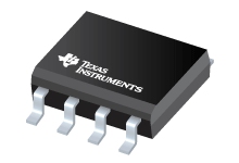
Texas Instruments
OP07CDR
|
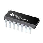
Texas Instruments
OPA4228PA
|
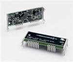
Texas Instruments
PTH08T220WAZT
|
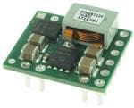
Texas Instruments
PTH08T220WAD
|
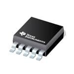
Texas Instruments
LM2595S-12
|
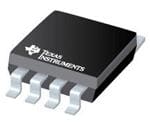
Texas Instruments
THS4011CDGNG4
|
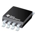
Texas Instruments
TPS77101DGKG4
|
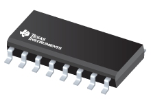
Texas Instruments
SN74CBT3257CPWG4
|
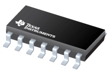
Texas Instruments
SN74HC74DG4
|
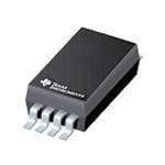
Texas Instruments
LM385PW-2-5
|
| Price |
|
$0.52 |
|
|
|
|
|
|
|
|
|
| RoHS |
|
Compliant |
Compliant |
Compliant |
Compliant |
Not Compliant |
Compliant |
Compliant |
Compliant |
Compliant |
Compliant |
| Lead Status |
|
No |
No |
No |
No |
No |
No |
No |
No |
Yes |
No |
| Output Current(Typ)(mA) |
|
|
|
|
|
|
110 |
|
|
|
|
| CMRR(Min)(dB) |
|
|
|
|
|
|
82 |
|
|
|
|
| Iq per channel(Max)(mA) |
|
|
|
|
|
|
9.5 |
|
|
|
|
| Offset Drift(Typ)(uV/C) |
|
|
|
|
|
|
15 |
|
|
|
|
| Total Supply Voltage(Max)(+5V=5, +/-5V=10) |
|
|
|
|
|
|
30 |
|
|
|
|
| Iq per channel(Typ)(mA) |
|
|
|
|
|
|
7.8 |
|
|
|
|
| Rating |
|
|
|
|
|
|
Catalog |
Catalog |
Catalog |
Catalog |
|
| Approx. Price (US$) |
|
|
|
|
|
|
1.99 | 1ku |
0.60 | 1ku |
0.18 | 1ku |
0.07 | 1ku |
|
| 3rd Harmonic(dBc) |
|
|
|
|
|
|
80 |
|
|
|
|
| Architecture |
|
|
|
|
|
|
Bipolar,Voltage FB |
|
|
|
|
| Total Supply Voltage(Min)(+5V=5, +/-5V=10) |
|
|
|
|
|
|
10 |
|
|
|
|
| Slew Rate(Typ)(V/us) |
|
|
|
|
|
|
310 |
|
|
|
|
| @ MHz |
|
|
|
|
|
|
1 |
|
|
|
|
| Acl, min spec gain(V/V) |
|
|
|
|
|
|
1 |
|
|
|
|
| Package Group |
|
|
|
|
|
|
MSOP-PowerPAD,SOIC |
VSSOP |
SOIC,SSOP,TSSOP,VQFN |
PDIP,SO,SSOP,SOIC,TSSOP |
|
| Input Bias Current(Max)(pA) |
|
|
|
|
|
|
6000000 |
|
|
|
|
| BW @ Acl(MHz) |
|
|
|
|
|
|
290 |
|
|
|
|
| 2nd Harmonic(dBc) |
|
|
|
|
|
|
80 |
|
|
|
|
| Package Size |
|
|
|
|
|
|
mm2 |
mm2 |
mm2 |
mm2 |
|
| GBW(Typ)(MHz) |
|
|
|
|
|
|
290 |
|
|
|
|
| Operating Temperature Range(C) |
|
|
|
|
|
|
-40 to 85,0 to 70 |
-40 to 125 |
-40 to 85 |
-40 to 85 |
|
| Vn at Flatband(Typ)(nV/rtHz) |
|
|
|
|
|
|
7.5 |
|
|
|
|
| Number of Channels(#) |
|
|
|
|
|
|
1 |
|
4 |
|
|
| Additional Features |
|
|
|
|
|
|
N/A |
|
Low Power |
|
|
| CMRR(Typ)(dB) |
|
|
|
|
|
|
110 |
|
|
|
|
| Vos (Offset Voltage @ 25C)(Max)(mV) |
|
|
|
|
|
|
6 |
|
|
|
|
| Rail-to-Rail |
|
|
|
|
|
|
No |
|
|
|
|
| Fixed Output Options(V) |
|
|
|
|
|
|
|
1.5,1.8,2.7,2.8,3.3,5 |
|
|
|
| Vout(Max)(V) |
|
|
|
|
|
|
|
5.5 |
|
|
|
| Iq(Typ)(mA) |
|
|
|
|
|
|
|
0.09 |
|
|
|
| Vin(Max)(V) |
|
|
|
|
|
|
|
10 |
|
|
|
| Vin(Min)(V) |
|
|
|
|
|
|
|
2.7 |
|
|
|
| Noise(uVrms) |
|
|
|
|
|
|
|
55 |
|
|
|
| Thermal Resistance JA(C/W) |
|
|
|
|
|
|
|
243 |
|
|
|
| Regulated Outputs(#) |
|
|
|
|
|
|
|
1 |
|
|
|
| Iout(Max)(A) |
|
|
|
|
|
|
|
0.15 |
|
|
|
| Vout(Min)(V) |
|
|
|
|
|
|
|
1.5 |
|
|
|
| Vdo(Typ)(mV) |
|
|
|
|
|
|
|
75 |
|
|
|
| Special Features |
|
|
|
|
|
|
|
Enable,Power Good |
|
|
|
| Output Capacitor Type |
|
|
|
|
|
|
|
Non-Ceramic |
|
|
|
| Accuracy(%) |
|
|
|
|
|
|
|
2 |
|
|
|
| Output Options |
|
|
|
|
|
|
|
Adjustable Output,Fixed Output |
|
|
|
| PSRR @ 100KHz(dB) |
|
|
|
|
|
|
|
26 |
|
|
|
| Configuration |
|
|
|
|
|
|
|
|
2 |
|
|
| VCC(Min)(V) |
|
|
|
|
|
|
|
|
4 |
2 |
|
| ICC(Max)(uA) |
|
|
|
|
|
|
|
|
3 |
|
|
| Bandwidth(MHz) |
|
|
|
|
|
|
|
|
200 |
|
|
| Vdd(Min)(V) |
|
|
|
|
|
|
|
|
4 |
|
|
| Input/Ouput Voltage(Max)(V) |
|
|
|
|
|
|
|
|
5.5 |
|
|
| Vdd(Max)(V) |
|
|
|
|
|
|
|
|
5.5 |
|
|
| Input/Ouput Voltage(Min)(V) |
|
|
|
|
|
|
|
|
0 |
|
|
| Input/Output Continuous Current(Max)(mA) |
|
|
|
|
|
|
|
|
128 |
|
|
| Supply Range(Max) |
|
|
|
|
|
|
|
|
5.5 |
|
|
| Ron(Max)(Ohms) |
|
|
|
|
|
|
|
|
12 |
|
|
| VCC(Max)(V) |
|
|
|
|
|
|
|
|
5.5 |
6 |
|
| Ron(Typ)(Ohms) |
|
|
|
|
|
|
|
|
3 |
|
|
| Bandwidth(Max)(MHz) |
|
|
|
|
|
|
|
|
200 |
|
|
| 3-State Output |
|
|
|
|
|
|
|
|
|
No |
|
| Voltage(Nom)(V) |
|
|
|
|
|
|
|
|
|
3.3,5 |
|
| Output Drive (IOL/IOH)(Max)(mA) |
|
|
|
|
|
|
|
|
|
5.2/-5.2 |
|
| ICC @ Nom Voltage(Max)(mA) |
|
|
|
|
|
|
|
|
|
0.04 |
|
| F @ Nom Voltage(Max)(Mhz) |
|
|
|
|
|
|
|
|
|
28 |
|
| Technology Family |
|
|
|
|
|
|
|
|
|
HC |
|
| Schmitt Trigger |
|
|
|
|
|
|
|
|
|
No |
|
| tpd @ Nom Voltage(Max)(ns) |
|
|
|
|
|
|
|
|
|
37 |
|
| Bits(#) |
|
|
|
|
|
|
|
|
|
2 |
|