|
|
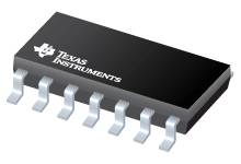
Texas Instruments
SN74AS1004ADRE4
|
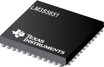
Texas Instruments
LM3S5651-IBZ80-C5
|
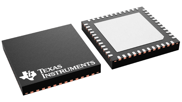
Texas Instruments
BQ500110RGZR
|
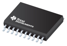
Texas Instruments
SN74LV373ATPWTE4
|
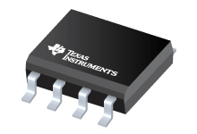
Texas Instruments
TLC2272IPWG4
|
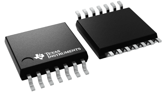
Texas Instruments
V62/04687-02YE
|
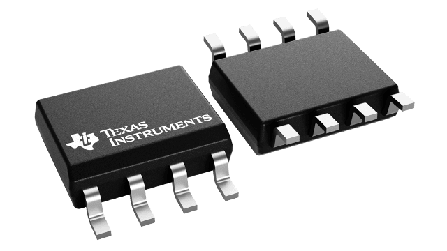
Texas Instruments
OPA134UA
|
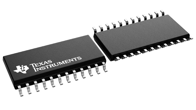
Texas Instruments
V62/09615-01XE
|
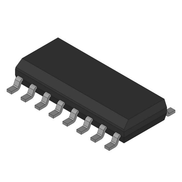
Texas Instruments
OPA3691IDR
|
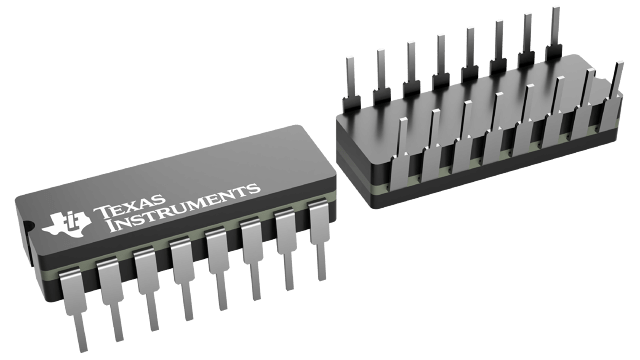
Texas Instruments
JM38510/66304BEA
|
| Price |
|
|
|
|
|
|
|
$1.76 |
|
|
|
| RoHS |
|
Compliant |
Compliant |
Yes |
Compliant |
Compliant |
Compliant |
Yes |
Compliant |
Yes |
No |
| Lead Status |
|
|
No |
Yes |
|
Yes |
See ti.com |
Yes |
Yes |
Yes |
No |
| Rating |
|
|
|
Catalog |
|
Catalog |
HiRel Enhanced Product |
Catalog |
HiRel Enhanced Product |
Catalog |
Military |
| Function |
|
|
|
Transmitter |
|
|
|
|
|
|
Counter |
| Package Group |
|
|
|
VQFN |
|
PDIP,SOIC,SO,TSSOP |
TSSOP |
PDIP,SOIC |
SOIC,TSSOP,VQFN |
SOIC,SSOP |
CDIP,LCCC |
| Estimated Package Size (WxL)(mm2) |
|
|
|
[pf]48VQFN[/pf] |
|
|
|
|
|
|
|
| Compliance |
|
|
|
WPC 1.0 |
|
|
|
|
|
|
|
| Vin(Typ)(V) |
|
|
|
19 |
|
|
|
|
|
|
|
| Approx. Price (US$) |
|
|
|
4.50 | 1ku |
|
0.68 | 1ku |
|
1.10 | 1ku |
|
3.40 | 1ku |
|
| Operating Temperature Range(C) |
|
|
|
-40 to 110 |
|
-40 to 125,0 to 70 |
-40 to 125 |
-40 to 85 |
-55 to 125 |
-40 to 85 |
-55 to 125 |
| Output Current(Typ)(mA) |
|
|
|
|
|
2.2 |
|
40 |
|
190 |
|
| CMRR(Typ)(dB) |
|
|
|
|
|
75 |
|
100 |
|
56 |
|
| Additional Features |
|
|
|
|
|
High Cload Drive |
|
Burr-Brown Audio |
|
Shutdown |
|
| Offset Drift(Typ)(uV/C) |
|
|
|
|
|
2 |
|
2 |
|
20 |
|
| CMRR(Min)(dB) |
|
|
|
|
|
70 |
|
86 |
|
52 |
|
| Total Supply Voltage(Max)(+5V=5, +/-5V=10) |
|
|
|
|
|
16 |
|
36 |
|
12 |
|
| Slew Rate(Typ)(V/us) |
|
|
|
|
|
3.6 |
|
20 |
|
2100 |
|
| Package Size |
|
|
|
|
|
mm2 |
mm2 |
mm2 |
mm2 |
|
mm2 |
| Iq per channel(Max)(mA) |
|
|
|
|
|
1.5 |
|
5 |
|
5.3 |
|
| Input Bias Current(Max)(pA) |
|
|
|
|
|
60 |
|
100 |
|
|
|
| Architecture |
|
|
|
|
|
CMOS |
|
FET |
|
Bipolar,Current FB |
|
| Number of Channels(#) |
|
|
|
|
|
2 |
|
1 |
|
3 |
|
| GBW(Typ)(MHz) |
|
|
|
|
|
2.18 |
|
8 |
|
280 |
|
| Vn at 1kHz(Typ)(nV/rtHz) |
|
|
|
|
|
9 |
|
8 |
|
|
|
| Total Supply Voltage(Min)(+5V=5, +/-5V=10) |
|
|
|
|
|
4.4 |
|
5 |
|
4 |
|
| Iq per channel(Typ)(mA) |
|
|
|
|
|
1.1 |
|
4 |
|
5.1 |
|
| Vos (Offset Voltage @ 25C)(Max)(mV) |
|
|
|
|
|
2.5 |
|
2 |
|
3 |
|
| Rail-to-Rail |
|
|
|
|
|
In to V-,Out |
|
No |
|
No |
|
| tpd @ Nom Voltage(Max)(ns) |
|
|
|
|
|
|
18 |
|
25.9,13.2,11.4,11.1 |
|
46 |
| F @ Nom Voltage(Max)(Mhz) |
|
|
|
|
|
|
70 |
|
100 |
|
28 |
| Schmitt Trigger |
|
|
|
|
|
|
No |
|
|
|
No |
| Output Type |
|
|
|
|
|
|
CMOS |
|
|
|
|
| Technology Family |
|
|
|
|
|
|
HC |
|
LVC |
|
HC |
| ICC @ Nom Voltage(Max)(mA) |
|
|
|
|
|
|
0.02 |
|
0.025 |
|
0.08 |
| Input Type |
|
|
|
|
|
|
CMOS |
|
|
|
|
| Bits(#) |
|
|
|
|
|
|
4 |
|
8 |
|
4 |
| VCC(Max)(V) |
|
|
|
|
|
|
6 |
|
5.5 |
|
6 |
| VCC(Min)(V) |
|
|
|
|
|
|
2 |
|
1.65 |
|
2 |
| Output Drive (IOL/IOH)(Max)(mA) |
|
|
|
|
|
|
4/-4 |
|
|
|
5.2/-5.2 |
| IIB(Max)(pA) |
|
|
|
|
|
|
|
100 |
|
|
|
| VCCB(Min)(V) |
|
|
|
|
|
|
|
|
1.65 |
|
|
| VCCB(Max)(V) |
|
|
|
|
|
|
|
|
5.5 |
|
|
| VCCA(Max)(V) |
|
|
|
|
|
|
|
|
5.5 |
|
|
| ICCA Static Current(mA) |
|
|
|
|
|
|
|
|
0.015 |
|
|
| ICCB Static Current(mA) |
|
|
|
|
|
|
|
|
0.015 |
|
|
| VCCA(Min)(V) |
|
|
|
|
|
|
|
|
1.65 |
|
|
| IIB(Max)(nA) |
|
|
|
|
|
|
|
|
|
35000 |
|
| Vn at Flatband(Typ)(nV/rtHz) |
|
|
|
|
|
|
|
|
|
1.7 |
|
| BW @ Acl(MHz) |
|
|
|
|
|
|
|
|
|
280 |
|
| @ MHz |
|
|
|
|
|
|
|
|
|
5 |
|
| 3rd Harmonic(dBc) |
|
|
|
|
|
|
|
|
|
74 |
|
| Acl, min spec gain(V/V) |
|
|
|
|
|
|
|
|
|
1 |
|
| 2nd Harmonic(dBc) |
|
|
|
|
|
|
|
|
|
70 |
|
| Package Size(mm2=WxL) |
|
|
|
|
|
|
|
|
|
[pf]16SSOP[/pf] |
|
| Voltage(Nom)(V) |
|
|
|
|
|
|
|
|
|
|
3.3,5 |
| Type |
|
|
|
|
|
|
|
|
|
|
Binary |