
108648-HMC732LC4B
Analog Devices Inc.
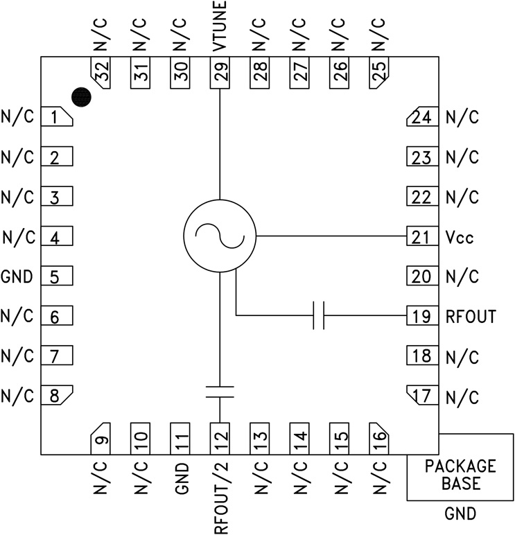
The HMC732LC4B is a wideband GaAs InGaP HBT MMIC Voltage Controlled Oscillator which incorporates the resonator, negative resistance device, and varactor diode. Output power and phase noise performance are excellent over temperature due to the oscillator's monolithic construction. The Vtune port accepts an analog tuning voltage from 0 to +23V. The HMC732LC4B VCO operates from a single +5V supply, consumes only 57 mA of current, and is housed in a RoHS compliant SMT package. This wideband VCO uniquely combines the attributes of ultra small size, low phase noise, low power consumption, and wide tuning range.APPLICATIONS Industrial/Medical Equipment Test & Measurement Equipment Military Radar, EW & ECM
| Distributor | SKU | Stock | MOQ | 1 | 10 | 50 | 100 | 1,000 | 10,000 |
|---|---|---|---|---|---|---|---|---|---|
| DigiKey | 1127-2329-ND | 2 | 1 | $1,530.14 | $1,530.14 | $1,530.14 | $1,530.14 | $1,530.14 | $1,530.14 |
| Analog Devices Inc | 108648-HMC732LC4B | 0 | $1,411.69 | $1,411.69 | $1,411.69 | $1,411.69 | $1,411.69 | $1,411.69 | |
| Arrow North American Components | 108648-HMC732LC4B | 0 | 1 | $1,514.99 | $1,499.84 | $1,470.00 | $1,455.30 | $1,412.07 | $1,397.95 |
| element14 APAC | 108648-HMC732LC4B | 4 | 1 | * $1,606.71 | * $1,606.71 | * $1,606.71 | * $1,606.71 | * $1,606.71 | * $1,606.71 |
| Farnell | 108648-HMC732LC4B | 4 | 1 | * $1,535.10 | * $1,535.10 | * $1,535.10 | * $1,535.10 | * $1,535.10 | * $1,535.10 |
| Mouser Electronics | 584-108648HMC732LC4B | 0 | 1 | $1,252.71 | $1,252.71 | $1,252.71 | $1,252.71 | $1,252.71 | $1,252.71 |
| Newark | 108648-HMC732LC4B | 4 | 1 | $1,471.50 | $1,471.50 | $1,471.50 | $1,471.50 | $1,471.50 | $1,471.50 |
| Verical Marketplace | 108648-HMC732LC4B | 2 | 1 | $1,455.05 | $1,455.05 | $1,455.05 | $1,455.05 | $1,455.05 | $1,455.05 |
110227-HMC511LP5
Analog Devices Inc.
The HMC511LP5(E) is a GaAs InGaP Heterojunction Bipolar Transistor (HBT) MMIC VCO. The HMC511LP5(E) integrates resonators, negative resistance devices, varactor diodes and feature a half frequency output. The VCO?s phase noise performance is excellent over temperature, shock, and process due to the oscillator?s monolithic structure. Power output is +13 dBm typical from a +5V supply. The voltage controlled oscillator is packaged in a leadless QFN 5x5 mm surface mount package, and requires no external matching components.APPLICATIONS VSAT Radio? Point-to-Point/Multi-Point Radio? Test Equipment & Industrial Controls? Military End-Use
| Distributor | SKU | Stock | MOQ | 1 | 10 | 50 | 100 | 1,000 | 10,000 |
|---|---|---|---|---|---|---|---|---|---|
| DigiKey | 1127-1913-ND | 1 | 1 | $597.84 | $10.00 | $10.00 | $10.00 | $10.00 | $10.00 |
| Analog Devices Inc | 110227-HMC511LP5 | 0 | $551.56 | $551.56 | $551.56 | $551.56 | $551.56 | $551.56 | |
| Arrow North American Components | 110227-HMC511LP5 | 0 | 1 | $591.92 | $586.00 | $574.34 | $568.60 | $551.71 | $546.19 |
| Mouser Electronics | 584-110227-HMC511LP5 | 3 | $485.38 | ||||||
| Verical Marketplace | 110227-HMC511LP5 | 15 | 1 | $568.50 | $568.50 | $568.50 | $568.50 | $568.50 | $568.50 |

110227-HMC735LP5
Analog Devices Inc.
The HMC735 is a GaAs InGaP Heterojunction Bipolar Transistor (HBT) MMIC VCO. The HMC735 integrates resonators, negative resistance devices, varactor diodes and features a divide-by-4 frequency output. The VCO's phase noise performance is excellent over temperature, shock, and process due to the oscillator's monolithic structure. Power output is +17 dBm typical from a +5V supply voltage. The prescaler function can be disabled to conserve current if not required. The voltage controlled oscillator is packaged in a leadless QFN 5x5 mm surface mount package, and requires no external matching components.APPLICATIONS Point-to-Multi-Point Radios Test Equipment & Industrial Controls SATCOM Military End-Use
| Distributor | SKU | Stock | MOQ | 1 | 10 | 50 | 100 | 1,000 | 10,000 |
|---|---|---|---|---|---|---|---|---|---|
| DigiKey | 505-110227-HMC735LP5-ND | 1 | 1 | $813.11 | $813.11 | $813.11 | $813.11 | $813.11 | $813.11 |
| Analog Devices Inc | 110227-HMC735LP5 | 0 | $750.18 | $750.18 | $750.18 | $750.18 | $750.18 | $750.18 | |
| Arrow North American Components | 110227-HMC735LP5 | 0 | 1 | $805.06 | $797.01 | $781.15 | $773.33 | $750.37 | $742.86 |
| Mouser Electronics | 584-110227-HMC735LP5 | 0 | 1 | $812.70 | $812.70 | $812.70 | $812.70 | $812.70 | $812.70 |
| Newark | 110227-HMC735LP5 | 0 | $635.05 | $635.05 | $635.05 | $635.05 | $635.05 | $635.05 | |
| Verical Marketplace | 110227-HMC735LP5 | 21 | 1 | $773.22 | $773.22 | $773.22 | $773.22 | $773.22 | $773.22 |

112261-HMC739LP4
Analog Devices Inc.
The HMC739 is a GaAs InGaP Heterojunction Bipolar Transistor (HBT) MMIC VCO. The HMC739 integrates a resonator, negative resistance device, varactor diode and divide-by-16 prescaler. The VCOs phase noise performance is excellent over temperature, shock, and process due to the oscillator's monolithic structure. Power output is +8 dBm typical from a 5V supply voltage. The voltage controlled oscillator is packaged in a low cost leadless QFN 4x4 mm surface mount package.APPLICATIONS Point-to-Point Radios Point-to-Multi-Point Radios/LMDS VSAT
| Distributor | SKU | Stock | MOQ | 1 | 10 | 50 | 100 | 1,000 | 10,000 |
|---|---|---|---|---|---|---|---|---|---|
| DigiKey | 1127-1914-ND | 2 | 1 | $864.67 | $864.67 | $864.67 | $864.67 | $864.67 | $864.67 |
| Analog Devices Inc | 112261-HMC739LP4 | 0 | $797.74 | $797.74 | $797.74 | $797.74 | $797.74 | $797.74 | |
| Arrow North American Components | 112261-HMC739LP4 | 0 | 1 | $783.25 | $783.25 | $783.25 | $783.25 | $783.25 | $783.25 |
| element14 APAC | 112261-HMC739LP4 | 4 | 1 | * $910.07 | * $910.07 | * $910.07 | * $910.07 | * $910.07 | * $910.07 |
| Farnell | 112261-HMC739LP4 | 4 | 1 | * $867.57 | * $867.57 | * $867.57 | * $867.57 | * $867.57 | * $867.57 |
| Mouser Electronics | 584-112261-HMC739LP4 | 0 | 1 | $864.27 | $864.27 | $864.27 | $864.27 | $864.27 | $864.27 |
| Newark | 112261-HMC739LP4 | 4 | 1 | $831.48 | $831.48 | $831.48 | $831.48 | $831.48 | $831.48 |
| Verical Marketplace | 112261-HMC739LP4 | 16 | 1 | $822.24 | $822.24 | $822.24 | $822.24 | $822.24 | $822.24 |

115739-HMC573LC3B
Analog Devices Inc.
The HMC573LC3B is a x2 active broadband frequency multiplier utilizing GaAs PHEMT technology in a leadless RoHS compliant SMT package. When driven by a +5 dBm signal, the multiplier provides +12 dBm typical output power from 8 to 22 GHz. The Fo and 3Fo isolations are >20 dBc and >25 dBc respectively at 16 GHz.The HMC573LC3B is ideal for use in LO multiplier chains for Pt to Pt & VSAT Radios yielding reduced parts count vs. traditional approaches. The low additive SSB Phase Noise of -134 dBc/Hz at 100 kHz offset helps maintain good system noise performance. The RoHS packaged HMC573LC3B eliminates the need for wire bonding, and allows the use of surface mount manufacturing techniques.APPLICATIONS Clock Generation Applications: SONET OC-192 & SDH STM-64 Point-to-Point & VSAT Radios Test Instrumentation Military & Space
| Distributor | SKU | Stock | MOQ | 1 | 10 | 50 | 100 | 1,000 | 10,000 |
|---|---|---|---|---|---|---|---|---|---|
| DigiKey | 505-115739-HMC573LC3B-ND | 1 | 1 | $350.84 | $350.04 | $350.04 | $350.04 | $350.04 | $350.04 |
| Analog Devices Inc | 115739-HMC573LC3B | 0 | $319.36 | $319.36 | $319.36 | $319.36 | $319.36 | $319.36 | |
| Arrow North American Components | 115739-HMC573LC3B | 0 | 1 | $316.19 | $313.03 | $306.80 | $303.73 | $294.71 | $291.77 |
| element14 APAC | 115739-HMC573LC3B | 5 | 1 | * $382.47 | * $382.47 | * $382.47 | * $382.47 | * $382.47 | * $382.47 |
| Farnell | 115739-HMC573LC3B | 5 | 1 | * $352.02 | * $352.02 | * $352.02 | * $352.02 | * $352.02 | * $352.02 |
| Mouser Electronics | 584-115739HMC573LC3B | 1 | 1 | $325.36 | $325.36 | $325.36 | $325.36 | $325.36 | $325.36 |
| Newark | 115739-HMC573LC3B | 5 | 1 | $436.83 | $436.83 | $436.83 | $436.83 | $436.83 | $436.83 |
| Verical Marketplace | 115739-HMC573LC3B | 9 | 1 | $329.17 | $329.17 | $329.17 | $329.17 | $329.17 | $329.17 |

122517-HMC744LC3
Analog Devices Inc.
The HMC744LC3?is a 1:2 Fanout Buffer designed to support data transmission rates up to 14 Gbps, and clock frequencies as high as 14 GHz.All differential inputs to the HMC744LC3 are CML and terminated on-chip with 50 Ohms to the positive supply, Vcc, and may be AC or DC coupled. The differential CML outputs are source terminated to 50 Ohms and may also be AC or DC coupled. Outputs can be connected directly to a 50 Ohm Vcc-terminated system, while DC blocking capacitors may be used if the terminating system is 50 Ohms to ground. The HMC744LC3 also features an output level control pin, VR, which allows for loss compensation or signal-level optimization. the HMC744LC3 operates from a single 3.3 V supply and is available in ROHS-compliant 3?3 mm SMT package.APPLICATIONS RF ATE Applications Broadband Test & Measurement Serial Data Transmission up to 14 Gbps Clock Buffering up to 14 GHz
| Distributor | SKU | Stock | MOQ | 1 | 10 | 50 | 100 | 1,000 | 10,000 |
|---|---|---|---|---|---|---|---|---|---|
| DigiKey | 505-122517-HMC744LC3-ND | 1 | 1 | $1,021.41 | $1,021.41 | $1,021.41 | $1,021.41 | $1,021.41 | $1,021.41 |
| Analog Devices Inc | 122517-HMC744LC3 | 0 | $904.64 | $904.64 | $904.64 | $904.64 | $904.64 | $904.64 | |
| Arrow North American Components | 122517-HMC744LC3 | 0 | 1 | $970.85 | $961.14 | $942.01 | $932.59 | $904.89 | $895.84 |
| Mouser Electronics | 584-122517-HMC744LC3 | 2 | 1 | $802.75 | $802.75 | $802.75 | $802.75 | $802.75 | $802.75 |
| Verical Marketplace | 122517-HMC744LC3 | 25 | 1 | $932.43 | $932.43 | $932.43 | $932.43 | $932.43 | $932.43 |

122517-HMC746LC3C
Analog Devices Inc.
The HMC746LC3C is an AND/NAND/OR/NOR function designed to support data transmission rates of up to 14 Gbps, and clock frequencies as high as 14 GHz. The HMC746LC3C may be easily configured to provide any of the following logic functions: AND, NAND, OR and NOR.All differential inputs to the HMC746LC3C are CML and terminated on-chip with 50 Ohms to the positive supply, Vcc, and may be AC or DC coupled. The differential CML outputs are source terminated to 50 Ohms and may also be AC or DC coupled. Outputs can be connected directly to a 50 Ohm Vcc-terminated system, while DC blocking capacitors may be used if the terminating system is 50 Ohms to ground. The HMC746LC3C also features an output level control pin, VR, which allows for loss compensation or signal-level optimization. the HMC746LC3C operates from a single 3.3 V supply and is available in ROHS-compliant 3x3 mm SMT package.APPLICATIONS RF ATE Applications Broadband Test & Measurement Serial Data Transmission up to 13 Gbps Digital Logic Systems up to 13 GHz NRZ-to-RZ Conversion
| Distributor | SKU | Stock | MOQ | 1 | 10 | 50 | 100 | 1,000 | 10,000 |
|---|---|---|---|---|---|---|---|---|---|
| DigiKey | 1127-2251-ND | 0 | 1 | $1,021.41 | $1,021.41 | $1,021.41 | $1,021.41 | $1,021.41 | $1,021.41 |
| Analog Devices Inc | 122517-HMC746LC3C | 0 | $904.64 | $904.64 | $904.64 | $904.64 | $904.64 | $904.64 | |
| Arrow North American Components | 122517-HMC746LC3C | 0 | 1 | $970.85 | $961.14 | $942.01 | $932.59 | $904.89 | $895.84 |
| Mouser Electronics | 584-122517HMC746LC3C | 4 | 1 | $975.23 | $975.23 | $975.23 | $975.23 | $975.23 | $975.23 |
| Newark | 122517-HMC746LC3C | 0 | $765.82 | $765.82 | $765.82 | $765.82 | $765.82 | $765.82 | |
| Verical Marketplace | 122517-HMC746LC3C | 17 | 1 | $932.43 | $1,005.16 | $991.93 | $991.93 | $991.93 | $991.93 |

123576-HMC729LC3C
Analog Devices Inc.
The HMC729LC3C is a T Flip-Flop w/Reset designed to support clock frequencies as high as 26 GHz. During normal operation, with the reset pin not asserted, the output toggles from its prior state on the positive edge of the clock. This results in a divide-by-two function of the clock input. Asserting the reset pin forces the Q output low regardless of the clock edge state (asynchronous reset assertion). Reversing the clock inputs allows for negative-edge triggered applications.All input signals to the HMC729LC3C are terminated with 50 to ground on-chip, and may be either AC or DC coupled. Outputs can be connected directly to a 50 terminated system, while DC blocking capacitors may be used if the terminating system is 50 to a non-ground DC voltage. The HMC729LC3C operates from a single -3.3V DC supply and is available in a ceramic RoHS compliant 3x3 mm SMT package.APPLICATIONS Serial Data Transmission up to 26 Gbps High Speed Frequency Divider (up to 26 GHz) Broadband Test & Measurement RF ATE Applications
| Distributor | SKU | Stock | MOQ | 1 | 10 | 50 | 100 | 1,000 | 10,000 |
|---|---|---|---|---|---|---|---|---|---|
| DigiKey | 505-123576-HMC729LC3C-ND | 2 | 1 | $977.00 | $977.00 | $977.00 | $977.00 | $977.00 | $977.00 |
| Analog Devices Inc | 123576-HMC729LC3C | 0 | $865.31 | $865.31 | $865.31 | $865.31 | $865.31 | $865.31 | |
| Arrow North American Components | 123576-HMC729LC3C | 0 | 1 | $928.63 | $919.35 | $901.05 | $892.04 | $865.55 | $856.89 |
| Mouser Electronics | 584-123576HMC729LC3C | 3 | 1 | $932.82 | $932.82 | $932.82 | $932.82 | $932.82 | $932.82 |
| Verical Marketplace | 123576-HMC729LC3C | 11 | 1 | $891.89 | $891.89 | $891.89 | $891.89 | $891.89 | $891.89 |

123815-HMC751LC4
Analog Devices Inc.
The HMC751 is a high dynamic range GaAs PHEMT MMIC Low Noise Amplifier (LNA) housed in a leadless 'Pb free' RoHS compliant SMT package. The HMC751 provides 25 dB of small signal gain, 2.2 dB of noise figure and output IP3 of +25 dBm. The P1dB output power of +13 dBm also enables the LNA to function as a LO driver for balanced, I/Q or image reject mixers. The HMC751 allows the use of surface mount manufacturing techniques.Applications Point-to-Point Radios Point-to-Multi-Point Radios & VSAT Test Equipment and Sensors Military
| Distributor | SKU | Stock | MOQ | 1 | 10 | 50 | 100 | 1,000 | 10,000 |
|---|---|---|---|---|---|---|---|---|---|
| DigiKey | 1127-2407-ND | 2 | 1 | $1,151.54 | $1,151.54 | $1,151.54 | $1,151.54 | $1,151.54 | $1,151.54 |
| Analog Devices Inc | 123815-HMC751LC4 | 0 | $1,062.41 | $1,062.41 | $1,062.41 | $1,062.41 | $1,062.41 | $1,062.41 | |
| Arrow North American Components | 123815-HMC751LC4 | 0 | 1 | $1,043.11 | $1,043.11 | $1,043.11 | $1,043.11 | $1,043.11 | $1,043.11 |
| element14 APAC | 123815-HMC751LC4 | 1 | 1 | * $1,252.71 | * $1,252.71 | * $1,252.71 | * $1,252.71 | * $1,252.71 | * $1,252.71 |
| Farnell | 123815-HMC751LC4 | 3 | 1 | * $1,155.40 | * $1,155.40 | * $1,155.40 | * $1,155.40 | * $1,155.40 | * $1,155.40 |
| Mouser Electronics | 584-123815-HMC751LC4 | 2 | 1 | $903.48 | $903.48 | $903.48 | $903.48 | $903.48 | $903.48 |
| Newark | 123815-HMC751LC4 | 3 | 1 | $1,107.36 | $1,107.36 | $1,107.36 | $1,107.36 | $1,107.36 | $1,107.36 |
| Verical Marketplace | 123815-HMC751LC4 | 21 | 1 | $1,095.04 | $1,095.04 | $1,095.04 | $1,095.04 | $1,095.04 | $1,095.04 |
| Win Source | 123815-HMC751LC4 | 2600 |

127283-HMC807LP6CE
Analog Devices Inc.
The HMC807LP6CE is a fully functioned Fractional-N Phase-Locked-Loop (PLL) with an Integrated Voltage Controlled Oscillator (VCO). The input reference frequency range is 100 kHz to 220 MHz while the advanced delta-sigma modulator design in the fractional PLL allows both ultra-fine step sizes and very low spurious products. The highly integrated structure provides excellent phase noise performance over temperature, shock and process. The HMC807LP6CE is packaged in a leadless QFN 6 x 6 mm surface mount package. The output power is 8 dBm typical, making the HMC807LP6CE ideal for driving the LO port of many of Hittite?s Hi Linearity and I/Q mixer products.For theory of operation and register map refer to the 'PLLs w/ Integrated VCO - Microwave VCOs' Operating Guide.Applications VSAT Radio Point-to-Point / Multi-Point Radio Test Equipment & Industrial Control Military End-Use Phased Array Applications
| Distributor | SKU | Stock | MOQ | 1 | 10 | 50 | 100 | 1,000 | 10,000 |
|---|---|---|---|---|---|---|---|---|---|
| DigiKey | 1127-2425-ND | 0 | $683.99 | ||||||
| Mouser Electronics | 584-127283HM807LP6CE | 2 | $740.68 |