| Distributor | SKU | Stock | MOQ | 1 | 10 | 50 | 100 | 1,000 | 10,000 |
|---|---|---|---|---|---|---|---|---|---|
| DigiKey | 1127-2239-ND | 0 | |||||||
| Mouser Electronics | 584-HMC995LP5GE | 0 | 1 | $46.01 | |||||
| Newark | HMC995LP5GE | 0 | 1 | $0.00 | $0.00 | $0.00 | $0.00 | $0.00 | $0.00 |
| Distributor | SKU | Stock | MOQ | 1 | 10 | 50 | 100 | 1,000 | 10,000 |
|---|---|---|---|---|---|---|---|---|---|
| DigiKey | HMC460LC5 | 1 | 1 | $1,230.45 | $217.02 | $207.30 | $194.00 | $194.00 | $194.00 |
| Analog Devices Inc | HMC460LC5 | 0 | $186.14 | $174.51 | $174.51 | $174.51 | $174.51 | $174.51 | |
| Arrow Asia | HMC460LC5 | 99 | 3 | $125.76 | $117.65 | $117.65 | $117.65 | $117.65 | |
| Arrow Europe | HMC460LC5 | 1 | 1 | $198.17 | $177.61 | $177.61 | $177.61 | $177.61 | $177.61 |
| Arrow North American Components | HMC460LC5 | 0 | 5 | $154.94 | $149.67 | $149.67 | $122.90 | $113.81 | |
| element14 APAC | HMC460LC5 | 7 | 1 | $342.91 | $303.53 | $303.53 | $303.53 | $303.53 | $303.53 |
| Farnell | HMC460LC5 | 7 | 1 | $196.89 | $167.73 | $167.73 | $167.73 | $167.73 | $167.73 |
| Mouser Electronics | HMC460LC5 | 653 | 1 | $182.62 | $174.89 | $168.46 | $165.89 | $165.54 | $165.54 |
| Newark | HMC460LC5 | 7 | 1 | $247.58 | $219.15 | $209.34 | $209.34 | $209.34 | $209.34 |
| Verical Marketplace | HMC460LC5 | 4 | 1 | $199.45 | $164.25 | $156.30 | $156.30 | $156.30 | $156.30 |
| Distributor | SKU | Stock | MOQ | 1 | 10 | 50 | 100 | 1,000 | 10,000 |
|---|---|---|---|---|---|---|---|---|---|
| DigiKey | ADF4113HVBCPZ | 0 | 1500 | $8.40 | $6.51 | $6.03 | $6.03 | $5.07 | $4.79 |
| Analog Devices Inc | ADF4113HVBCPZ | 0 | $7.72 | $6.97 | $6.65 | $6.65 | $6.65 | $6.65 | |
| Arrow North American Components | ADF4113HVBCPZ | 78 | 142 | $6.20 | $5.61 | $4.99 | $4.66 | $4.07 | $4.07 |
| element14 APAC | ADF4113HVBCPZ | 28 | 1 | $8.58 | $7.71 | $6.82 | $6.48 | $6.48 | $6.48 |
| Farnell | ADF4113HVBCPZ | 28 | 1 | $3.76 | $3.11 | $2.79 | $2.79 | $2.79 | $2.79 |
| Mouser Electronics | ADF4113HVBCPZ | 143 | 1 | $8.15 | $6.32 | $4.90 | $4.41 | $3.98 | $3.98 |
| Newark | ADF4113HVBCPZ | 31 | 1 | $6.28 | $5.67 | $4.95 | $4.48 | $4.48 | $4.48 |
| Verical Marketplace | ADF4113HVBCPZ | 78 | 78 | $5.62 | $5.00 | $4.66 | $4.07 | $4.07 | |
| Win Source | ADF4113HVBCPZ | 4700 |

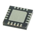
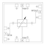
HMC370LP4E
Analog Devices Inc.
FREQ MULTIPLIER, 14.4-16.4GHZ, QFN-24; F; FREQ MULTIPLIER, 14.4-16.4GHZ, QFN-24; Frequency Min: 14.4GHz; Frequency Max: 16.4GHz; Supply Voltage Min: 4.5V; Supply Voltage Max: 5.5V; RF IC Case Style: QFN; No. of Pins: 24Pins; Operating Temperature Min: -40 C; Packaging: Each
| Distributor | SKU | Stock | MOQ | 1 | 10 | 50 | 100 | 1,000 | 10,000 |
|---|---|---|---|---|---|---|---|---|---|
| DigiKey | HMC370LP4E | 480 | 1 | $42.56 | $34.77 | $32.83 | $30.69 | $29.06 | $29.06 |
| Analog Devices Inc | HMC370LP4E | 0 | $38.89 | $35.87 | $34.26 | $30.63 | $29.22 | $29.22 | |
| Arrow North American Components | HMC370LP4E | 1 | 23 | $33.40 | $30.60 | $26.66 | $26.66 | $26.66 | $26.66 |
| element14 APAC | HMC370LP4E | 18 | 1 | $60.72 | $49.61 | $46.85 | $43.79 | $42.34 | $42.34 |
| Farnell | HMC370LP4E | 20 | 1 | $32.01 | $27.45 | $26.22 | $25.70 | $25.17 | $25.17 |
| Mouser Electronics | HMC370LP4E | 508 | 1 | $40.35 | $31.70 | $28.77 | $27.06 | $27.06 | $27.06 |
| Newark | HMC370LP4E | 18 | 1 | $43.01 | $33.41 | $31.40 | $31.40 | $31.40 | $31.40 |
| Verical Marketplace | HMC370LP4E | 1 | 1 | $26.66 | $30.60 | $28.33 | $28.33 | $28.33 | $28.33 |
| Win Source | HMC370LP4E | 51 | 2 |
| Distributor | SKU | Stock | MOQ | 1 | 10 | 50 | 100 | 1,000 | 10,000 |
|---|---|---|---|---|---|---|---|---|---|
| DigiKey | HMC453QS16GE | 0 | 500 | $22.84 | $17.06 | $15.72 | $14.37 | $16.10 | $16.10 |
| Analog Devices Inc | HMC453QS16GE | 0 | $19.71 | $18.20 | $16.68 | $15.42 | $15.17 | $15.17 | |
| Arrow North American Components | HMC453QS16GE | 0 | 44 | $14.77 | $11.34 | $14.47 | $0.00 | ||
| element14 APAC | HMC453QS16GE | 14 | 1 | * $25.59 | * $25.08 | * $24.57 | * $24.06 | * $23.55 | * $23.55 |
| Farnell | HMC453QS16GE | 24 | 1 | * $25.57 | * $20.00 | * $19.11 | * $17.08 | * $16.74 | * $16.74 |
| Mouser Electronics | HMC453QS16GE | 480 | 1 | $21.56 | $19.88 | $17.57 | $16.87 | $14.52 | $14.38 |
| Newark | HMC453QS16GE | 14 | 1 | $23.53 | $20.59 | $18.13 | $18.13 | $18.13 | $18.13 |
| Win Source | HMC453QS16GE | 2100 | 2 |
| Distributor | SKU | Stock | MOQ | 1 | 10 | 50 | 100 | 1,000 | 10,000 |
|---|---|---|---|---|---|---|---|---|---|
| DigiKey | 1127-2752-ND | 0 | 2 | $1.00 | $92.07 | $86.46 | $45.06 | $45.06 | $45.06 |
| Mouser Electronics | 584-HMC-VVD106 | 0 | 1 | ||||||
| Newark | HMC-VVD106 | 0 | $71.02 | $71.02 | $65.98 | $63.81 | $61.65 | $61.65 |
| Distributor | SKU | Stock | MOQ | 1 | 10 | 50 | 100 | 1,000 | 10,000 |
|---|---|---|---|---|---|---|---|---|---|
| DigiKey | 1127-1416-2-ND | 0 | $3.89 | $3.89 | $2.50 | $2.34 | $1.94 | $1.75 | |
| Mouser Electronics | 584-HMC479MP86E | 0 | 1 | ||||||
| Win Source | HMC479MP86E | 10600 | 17 |
| Distributor | SKU | Stock | MOQ | 1 | 10 | 50 | 100 | 1,000 | 10,000 |
|---|---|---|---|---|---|---|---|---|---|
| DigiKey | 505-HMC558ALC3B-ND | 380 | 1 | $71.57 | $62.84 | $59.82 | $55.68 | $46.34 | $46.34 |
| Mouser Electronics | 584-HMC558 | 0 | 1 | $18.49 | |||||
| Newark | HMC558 | 0 | 50 | $0.00 | $0.00 | $0.00 | $0.00 | $0.00 | $0.00 |
| Win Source | HMC558 | 1180 | 1 |
| Distributor | SKU | Stock | MOQ | 1 | 10 | 50 | 100 | 1,000 | 10,000 |
|---|---|---|---|---|---|---|---|---|---|
| DigiKey | 1127-3305-ND | 0 | $354.61 | $190.02 | $190.02 | $190.02 | $190.02 | ||
| Arrow North American Components | HMC-ABH241 | 0 | 25 | $85.70 | $85.70 | $111.23 | $111.23 | $104.97 | $89.85 |
| Mouser Electronics | 584-HMC-ABH241 | 0 | 25 | ||||||
| Newark | HMC-ABH241 | 0 | $96.05 | $96.05 | $96.05 | $96.05 | $96.05 | $96.05 | |
| Verical Marketplace | HMC-ABH241 | 150 | 25 | $85.70 | $85.70 | $85.70 | $85.70 | ||
| Win Source | HMC-ABH241 | 50 | 1 |
| Distributor | SKU | Stock | MOQ | 1 | 10 | 50 | 100 | 1,000 | 10,000 |
|---|---|---|---|---|---|---|---|---|---|
| DigiKey | HMC-C031-ND | 0 | |||||||
| Arrow North American Components | HMC-C031 | 0 | 1 | $2,341.58 | $2,311.18 | $2,311.18 | $2,166.59 | $2,126.18 | $2,126.18 |
| Mouser Electronics | 584-HMC-C031 | 0 | 1 | $0.00 | |||||
| Newark | HMC-C031 | 0 | $2,867.42 | $2,649.64 | $2,558.90 | $2,558.90 | $2,558.90 | $2,558.90 | |
| Verical Marketplace | HMC-C031 | 2 | 1 | $2,341.58 | $2,341.58 | $2,341.58 | $2,341.58 | $2,341.58 | $2,341.58 |